
ScopePhi Interposer Blueprint
Why you'd want it
The 28-layer board that connects the ScopePhi die's fine ball grid to the much wider grid of the card.
- Who it's for: board and packaging teams that need the ScopePhi interposer design ready for an HDI fab.
- The problem it solves: moves 0.8 mm die pitch to 2.0 mm board pitch; 162 of 165 signals routed.
- What you get: KiCad file, Gerbers, drill, test netlist and fab notes on encrypted Blu-ray; fab fees not included.
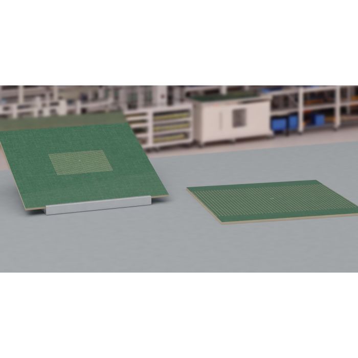
In between the die and the board sits a third piece that most readers have never looked at closely: the interposer. It is a short, thick slab of printed-circuit material whose only job is translation. The ScopePhi die wants to talk to the outside world on a grid of 1,536 pads at a pitch of 0.8 millimetres — because that is the pitch its 858 square millimetres can afford to spend. The ScopePhi Card wants to receive the same 1,536 signals, but at a pitch of 2 millimetres — because that is the pitch a datacenter-grade PCIe board can be built and tested at without the escape routing becoming impossible to debug.
The interposer is what makes those two numbers meet. On the top face it is 37.6 by 24.8 millimetres and lays out a 48-by-32 grid of pads at 0.8 millimetres apart — the die's dialect. On the bottom face it is 94 by 62 millimetres and lays out the same 48-by-32 grid at 2 millimetres apart — the board's dialect. In between, inside the slab, 28 copper layers (22 of them for signal) carry every real net from one grid to the other, with microvias small enough to pass through 0.1-millimetre openings and stacks of microvias large enough that the signal does not meander through 300 millimetres of trace to go 10 millimetres across the chip.
There are 165 real signal nets that need to make it from the die to the card: 73 for the DDR3 memory, 64 for the PCIe host interface, 64 for the QBeam optical pairs that carry bytes between layers at light speed, and 36 for management (SMBus, JTAG, SPI, UART, charge, power). Four hundred and forty-one of the die's remaining pins carry high-speed I/O that we deliberately parked inside the chip — tied to ground with fresh microvia stitches — because they are spare capacity for a future respin and routing them out would just waste layers. Two hundred and eighty-two more management pins got the same treatment, for the same reason. That decision — what to leave on the chip — is what unblocked the routing of the real signals.
At the end of the session on 2026-10-24, 162 of the 165 real signal escapes were closed, zero shorts, zero mask bridges, with the last 3 outer-ring signals on rings 0 and 1 waiting on either one more signal-layer bump or a short manual GUI pass. Every production artifact is already generated: Gerbers, Excellon drill, IPC-2581, STEP, IPC-D-356 netlist, PDF layer book, top-and-bottom renders, and the fab-notes README written for Advanced Circuits — who have blind + buried + stacked microvia confirmed in their current capability list.
A patron pledging on the interposer is pledging on a piece that already exists in file form. The pledge covers the finishing pass on the last three signals, the fabrication of the HDI panels at Advanced Circuits, the test coupons that come with any new HDI build, and the handoff. When first interposers come back, every patron gets their AES-256-encrypted Blu-ray with the full build on it — the KiCad file, every artifact above, and the fab-notes exactly as submitted. Non-exclusive on purpose.
ScopePhi Interposer Blueprint
The 1,536-ball interposer that bonds the ScopePhi die to the ScopePhi Card. Its job is to translate between two very different ball pitches — the die's 0.8 mm pitch on one side, the board's 2.0 mm pitch on the other — without losing a signal in the middle. 28-layer HDI with 22 signal layers, blind + buried + stacked microvia, routed to 162 of 165 real signal nets.
Spec.
- Die side: 1,536 pads, 48×32 array, 0.800 mm pitch, 37.60 × 24.80 mm
- Board side: 1,536 pads, 48×32 array, 2.000 mm pitch, 94.00 × 62.00 mm
- Stackup: TOP, GND1, SIG1–18, PWR1, PWR2, GND2, SIG19–22, BOTTOM (28 copper layers, 22 signal)
- Microvia 0.20/0.10 mm; blind via 0.40/0.20 mm; stacked microvia confirmed in Advanced Circuits capability
- 0.075 mm track width; 0.125 mm netclass clearance
- HDI ruleset aligned to the real geometry (not stock defaults)
- Rails placed on their planes: GND→GND1+GND2, APH_VDD_CORE→PWR1, 1V0→PWR2
- 441 APH_HSIO + 282 APH_MGMT_GPIO spare balls intentionally parked (tied to GND, fresh microvia stitches) — what unblocked the escape routing on the real signals
- Real signal breakdown: 73 DDR3, 64 PCIe, 64 QBeam RX/TX, 36 management
Routing state. 162 of 165 real signal escapes closed; the last three outer-ring signals on rings 0–1 close with one more signal layer bump (24→28 handled; 28→32 available) or a manual GUI pass. Zero shorts. Zero mask bridges. All production artifacts generated and sitting in production-pack-28layer-v3/.
Deliverable (ships now).
- KiCad PCB file (
autophi-1536-interposer-v3.kicad_pcb) - Gerber RS-274X set
- Excellon drill
- IPC-2581 (full build-dataset)
- 3D STEP for mechanical fit
- Pick-and-place CSV
- IPC-D-356 netlist for bare-board test
- PDF layer book
- Top and bottom renders
- Fab-notes README for Advanced Circuits
Blind + buried + stacked microvias confirmed in Advanced Circuits capability as of 2026-10-24. Patent pending: USPTO 19/835,210 (umbrella).
Non-exclusive on purpose. Multiple patrons may pledge; each receives their own copy; the IP, package program and routing pipeline stay with the inventor.
Inventor. Christopher Gabriel Brown (cri-one.com), sole inventor.
Exhaustive deliverable checklist
- ☐ KiCad PCB file (
autophi-1536-interposer-v3.kicad_pcb) - ☐ Gerber RS-274X set (every copper, mask, silkscreen and paste layer, all 28 layers)
- ☐ Excellon drill files (microvia + blind + buried + through)
- ☐ IPC-2581 (full build dataset)
- ☐ 3D STEP for mechanical fit
- ☐ Pick-and-place CSV
- ☐ IPC-D-356 netlist for bare-board test
- ☐ PDF layer book (all 28 layers rendered)
- ☐ Top-face and bottom-face renders
- ☐ Pinmap: 1,536 die-side pads at 0.800 mm pitch; 1,536 board-side pads at 2.000 mm pitch; 48×32 arrays both sides
- ☐ Stackup spec: TOP, GND1, SIG1–18, PWR1, PWR2, GND2, SIG19–22, BOTTOM (28 copper, 22 signal)
- ☐ HDI ruleset aligned to the real geometry: microvia 0.20/0.10 mm; blind via 0.40/0.20 mm; 0.075 mm track; 0.125 mm netclass clearance
- ☐ Rail placement: GND→GND1+GND2, APH_VDD_CORE→PWR1, 1V0→PWR2
- ☐ Spare-lane parking record: 441 APH_HSIO + 282 APH_MGMT_GPIO balls tied to GND with fresh microvia stitches
- ☐ Real signal breakdown: 73 DDR3, 64 PCIe, 64 QBeam RX/TX, 36 management (SMBus/JTAG/SPI/UART/CHG/PWR)
- ☐ Routing state: 162 of 165 real signal escapes closed; zero shorts; zero mask bridges
- ☐ Open-item inventory: 3 outer-ring signals on rings 0–1 pending one manual GUI pass (or one more layer bump)
- ☐ Advanced Circuits fab-notes README (blind + buried + stacked microvia confirmed in current capability list as of 2026-10-24)
- ☐ AES-256 encryption of the Blu-ray and the key-handoff procedure
- ☐ Patent filing: USPTO 19/835,210 (umbrella)
What could go wrong, and what we have done about it
- 3 outer-ring signals still open. Each closes with either a short manual GUI pass or one more signal-layer bump (24→28 is already handled; 28→32 is available in the Advanced Circuits capability list). Listed openly rather than hidden; a buyer sees the exact remaining work.
- HDI yield on a 28-copper-layer board. Advanced Circuits confirmed blind + buried + stacked microvia in their current capability list as of 2026-10-24. The HDI ruleset in the deliverable is aligned to the real geometry, not to stock defaults that would blow the DRC.
- Microvia stack reliability. Stackup places vias on their planes (GND1/GND2 for ground, PWR1/PWR2 for the two rails). Stacked microvias are standard in current Advanced Circuits capability.
- Pitch translation from 0.800 mm to 2.000 mm. Covered by the 22 signal layers in the stackup. The whole point of the interposer is to spend layer count on the pitch move so the carrier board does not have to.
- Spare-lane routing debt. 441 APH_HSIO + 282 APH_MGMT_GPIO balls are parked inside the chip with fresh microvia stitches to GND. The decision to park these inside the chip (rather than route them out) is what unblocked the escape routing on the 165 real signals.
- Panel size and tooling at the fab. The 94 × 62 mm board-side footprint sits within Advanced Circuits' standard panelization. No custom tooling fee is baked into the pledge.
- Bare-board test coverage. IPC-D-356 netlist ships with the package so the fab's flying-probe or bed-of-nails test rig verifies every net before populate.
- Mechanical fit on the carrier board. 3D STEP ships with the package for mechanical fit against the ScopePhi Card drawing.
- Fab fees are not in the pledge. The pledge covers the engineering handoff — the AES-256-encrypted Blu-ray with the file set (Gerbers, Excellon drill, IPC-2581, STEP, pick-and-place, IPC-D-356 netlist, PDF layer book, fab-notes README). Advanced Circuits panels (or any equivalent HDI fab) are ordered by the patron directly at the fab's standard pricing.
- Two paths at Advanced Circuits, patron picks. Either (a) order 28-layer HDI panels only, against the Gerbers and IPC-2581 in the production pack — standard HDI pricing, no design involvement from AC; or (b) hire AC's Design Services to close the last 3 outer-ring signals on the live board file and then fab the panels in the same engagement — turnkey from file to populated interposer. Both are at AC's own standard pricing, both sit outside this pledge.
- IP escape. AES-256-encrypted Blu-ray with keyed handoff. The IP, package program and routing pipeline stay with the inventor; patrons receive a copy, not control.
Tests and measurements (internal, in the deliverable)
- 2026-10-24 cleanup session results: V1 interposer at 40-autophi-bga256 from 1,655 DRC violations cleaned to a 329-unconnected / zero-shorts baseline; that clean state is V2's starting point in its own numbered project (V1 kept as history)
- V2 (24-layer): 24 copper layers, 18 signal layers, 155 of 165 real signal escapes closed, production pack at
production-pack-24layer/ - V3 (28-layer): 28 copper layers, 22 signal layers, 162 of 165 real signal escapes closed, production pack at
production-pack-28layer-v3/, zero shorts - Rails verified placed on their planes: GND → GND1 + GND2, APH_VDD_CORE → PWR1, 1V0 → PWR2
- Spare-lane parking verified: 441 APH_HSIO + 282 APH_MGMT_GPIO balls tied to GND with fresh microvia stitches (the decision that unblocked the escape routing)
- HDI ruleset aligned to the real geometry (microvia 0.20/0.10 mm, 0.05 mm annular, 0.45 mm edge clearance, 0.125 mm netclass clearance), not stock defaults that would blow the DRC
- Advanced Circuits capability check (2026-10-24): blind + buried + stacked microvia confirmed in their current capability list
- Production handoff pack generated: Gerbers, Excellon drill, IPC-2581, 3D STEP, pick-and-place, IPC-D-356 netlist, PDF layer book, top-and-bottom renders, fab-notes README
References
- USPTO Patent Center — patentcenter.uspto.gov — filing 19/835,210 (umbrella)
- Advanced Circuits / AdvancedPCB / APCT (target HDI fab, blind + buried + stacked microvia capability) — advancedpcb.com (Design Services at advancedpcb.com → Design Services)
- IPC-2581 industry exchange format (full build dataset) — ipc2581.com
- IPC-D-356 bare-board test netlist standard — ipc.org
- KiCad EDA (the interposer is drawn in KiCad) — kicad.org
Also patent-pending under Quantum-Reactor-Scale. The compute-core architecture of this product is additionally covered by U.S. patent-pending applications 19/865,419 and 19/865,443 (filed 2026-11-06), with the chip-scale instantiation available as QRS-116 Compute Core Blueprint, and the reactor-scale embodiments available as QRS-117 Quantum Electric Reactor Blueprint (electricity-primary) and QRS-118 Compute Reactor Blueprint (compute-primary).
-
-
-
 PCIe8 Standard Performance
PCIe 8.0 storage chips sharing work across a data center.
$2,000,000,000.00 -
 ScopePhi Performance IC Blueprint
The two-reticle ScopePhi: one larger stitched die.
$216,000,000,000.00
-
 OFFICE-RAG — Fundamentals for Working With AI
Stop re-explaining yourself to your AI every morning.
$24.99 -
 Private Energy Farms
A concentrated-solar building, explained in a full engineering book.
$727,000,000.00