51-pcie8-standard - Performance
Valuation
Generous asset valuation: $60,000,000,000. The listed price is the platform maximum; acquisition at valuation is handled by direct enquiry.
51 — PCIe 8.0 Standard, Performance (Cri-One PCIe 8.0 SSD — Scale-Out)
Master index of all projects: PROJECTS_INDEX.
Sibling: 50-pcie8-standard — the secure-storage anchor (CS-50). This project is its scale-out + performance variant (CS-51).
Last edited: 2026-06-18
Status: L0 (Concept / Roadmap) — scaffold, no RTL bring-up yet; CS-50 substrate inherited.
Inventor: Christopher Gabriel Brown
Contact: crioneaka@outlook.com
What This Is
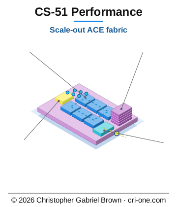
CS-51 is the scale-out and performance member of the AutoPhi computational-storage
family. It rides the same patent substrate as CS-50 (the secure-storage anchor,
USPTO Application 19/710,460, filed 2026-06-17) and adds:
- Multi-channel FTL parallelism — N parallel command pipes into the same FTL fabric
instead of one. The single-port arbiter of CS-50 generalises to an N-port arbiter
with the same reserved-CID semantics, so the patent claims read straight through.
- Scale-out AutoPhi Compute Engine (ACE) — multiple ACE instances on-die, each
consuming a stripe of the physical-page-tweaked plaintext stream. Designed for
the workloads CS-50 was already targeting (analytics, AI-pipeline preprocessing,
log search) at fleet scale.
- Peer arbitration between dies — CS-51 chips share work over a PCIe peer-to-peer
or CXL-like fabric. Host issues one vendor-opcode doorbell; the fabric splits the
result-reduction across N CS-51 endpoints and synthesises a single completion-queue
event back to the host.
- AI-pipeline preprocessing target — sustained streaming reduction over very large
datasets without round-tripping plaintext through host DRAM.
CS-51 is patent-pending under the CS-50 substrate; broader CS-51-specific claims
covering multi-channel parallelism and peer arbitration are scoped for a follow-on
non-provisional filing.
Relationship to CS-50
What's in this package
Quickstart
cd cri-one-pcie8-ssd-performance/ cat architecture.md # The scale-out diagram cat STATUS.md # What's stubbed vs. designed vs. RTL cd wonderphi-driver/hardware ls autophi_*scaleout*.v # New scale-out RTL stubs
Not yet
- No filed patent specific to CS-51 (the substrate is covered by CS-50's filing).
- No passing testbenches yet — every Verilog file in
cri-one-pcie8-ssd-performance/wonderphi-driver/hardware/is a stub. - No live store product. Acquisition tiers are deferred until L1 (working sim + passing testbenches).
License
See LICENSE (inherited from CS-50 — same terms apply to the CS-51 scaffold).
Invention Depositions — Project 50 (WonderPhi AES)
> Provenance / conceptual framing, not derivable from the code. Captured 2026-06-17.
>
> These are the 2017 Invent Deposition entries (one dated 2015) from the
> inventor's master sheet 1 light trigger.txt that document the **prior
> conception roots of this device — a secured PCIe 8.0 NVMe SSD (WonderPhi
> AES**). They establish when the ideas were written down and publicly offered,
> supporting the AutoPhi continuation-in-part family (parent U.S. 18/370,908).
What this is (and is not)
This file ties WonderPhi AES back to dated 2015–2017 disclosures. It is
provenance evidence, in the "first to market" sense:
- **First to market = a documented public-offering / conception record, NOT a
determination of patent priority** (the U.S. is first-to-file).
- Say patent-pending, never "patented." This is a design package, not
shipping silicon (PLAYBOOK §7).
- Verify any coverage claim against
../PATENT_PORTFOLIO.md
before relying on it.
Each entry quotes the 2017 text verbatim (deposition # = entry_num in the
master sheet) and maps it to the concrete part of this package it anticipates.
Source of record: the Invent Depositions book (ISBN 9781979767897, CreateSpace,
shipped 2017-11-24); full text in 1 light trigger.txt (1,757 entries).
1 · Solid-state storage substrate — the SSD itself
2 · The microSD RAID0 array — this project's literal media
3 · Vertical / stacked / layered 3D chip — NAND stack + layered controller
4 · Encryption / secured chip — WonderPhi AES (Commandment VIII)
5 · Compute — the AutoPhi Compute Engine (ACE)
The 2026-06-17 pivot makes this a computational-storage chip: an on-die
programmable compute core (ACE — VOXEL / SCAN / XFORM) that runs near the data.
Its 2017 roots:
(ACE's VOXEL op draws on the AutoPhi Voxel-processor lineage elsewhere in the
portfolio; storage roots are in §1–§3, encryption roots in §4.)
Earliest dated roots & priority story
- #618 is marked 2015 in the master sheet; the rest are 2017. Together they
place documented conception of a **secured, solid-state, RAID/stacked,
encrypted storage device at 2015–2017** — well before this PCIe 8.0
package and consistent with the AutoPhi CIP family (parent 18/370,908).
- These are conception/public-offering markers, not filed claims. For the
continuation-in-part argument, pair them with the third-party sweep in
PRIOR_ART_QUERIES.md and the canonical scope in ../PATENT_PORTFOLIO.md.
See also
1 light trigger.txt— the master deposition sheet (source; 1,757 entries)WONDERPHI_LINEAGE.md— what WonderPhi AES isPRIOR_ART_QUERIES.md— third-party prior-art sweepPLAYBOOK.md— identity, acquisition tiers, compliance rules
Patent audit findings — what's filed, what isn't, what's missed
> Investigation performed 2026-06-18 while Chris stepped out.
> Source: the 25 files at C:\Users\crione\Chris\special\ Chris pointed me at.
> Read me first; the answer to "do I need to file again" changed.
TL;DR — the short answer changed
You already have an umbrella filed for the CS-51 substrate work. I missed
this earlier. Read on for what it does and doesn't cover.
The big miss — CGB Framework is already filed
USPTO Application 19/693,405 ("Unified Mathematical-Deposition Framework
and Voxel-Computing System for Computer-Aided Derivation of Multi-Domain
Engineering Design Parameters")
- Filed: 2026-05-30
- Confirmation No.: 5107
- Patent Center No.: 76837851
- Type: Non-provisional utility
- 20 claims (3 independent + 17 dependent)
- Pro se (self-filed)
- Foreign filing deadline: 2027-05-30 — PCT or direct foreign-Paris-Convention
- Filing package:
C:\Users\crione\Chris\special\CGB-Patent-Filing-Package\patent-build\
What this umbrella covers (and doesn't)
Covers — the framework method:
- A Deposition Library of 10 cross-domain mathematical kernels
- A Voxel-Computing Substrate (mesh of compute nodes, π-locked coupling via Basel identity)
- A Derivation Engine that selects kernels, binds variables, and emits manufacturable specs
- 45 portfolio products explicitly named as embodiments
- Worked example: Autocar electromagnetic torque-plate stack (Deposition 1, Harmonic Decay) — measured within 2.3%
The 10 Depositions:
AutoPhi family explicitly named under Deposition 3 (Voxel Resonance):
- Projects 18, 21, 23, 24, 26 — AutoPhi Computing Ecosystem
- Project 30 — AutoPhi On-Demand Three
- Project 31 — AutoPhi Electromagnetic IC
- Project 45 — V19 Master Library
Does NOT cover (yet):
- Project 50 — PCIe 8.0 Standard / CS-50 (filed separately as 19/710,460 on 2026-06-17)
- Project 51 — CS-51 Performance variant (no filing)
- Project 42 — Software for Data (references 19/540,453 only, with "method-claim filing in preparation")
- The CS-51-specific new matter: N-port arbiter, AI-pipeline kernels (VECTOR_DOT/TOPK/EMBED_LOOKUP/SOFTMAX/ARGMAX), UCIe chiplet topology, peer arbitration, post-quantum hybrid AES wrap, attestation surface, scenario-on-die
But the spec text says explicitly: *"Remaining project numbers are reserved
embodiments to be slotted as their specifications are finalized."* That gives
you a slot for CS-50 and CS-51 as future embodiments of the framework.
The CHILD application is already drafted
Inside the filing package: CHILD-AutoPhi-V19.docx + .pdf (170 KB / 162 KB).
This is a divisional/continuation child application for AutoPhi V19 specifically, ready to file off 19/693,405 as the first device child.
The strategy memo says (verbatim):
> *"One issued patent cannot legally claim 45 distinct inventions, so the plan
> is: one broad 'parent' application on the framework, then device 'children'
> later... Prioritize by enablement strength."*
Tier 1 children (priority order):
1. AutoPhi / Project 45 (V19) — D3 Voxel Resonance — already drafted as CHILD
2. Autocar — D1 Harmonic Decay — measured-performance worked example
Tier 2 children: Quantum Battery / Electric Jet (D8), Microwave Nuclear Recycler (D6), Comms Satellite NCS-19 (D4)
Tier 3: Everything else, or defensively publish
So where does CS-51 fit?
CS-51 (and CS-50, and Software for Data) are NOT in the prepared children list.
They were added to the portfolio after the CGB Framework was filed (CS-50
filed 17 days later as a separate application; CS-51 created today).
Your best filing options for CS-51, ranked:
My recommendation: option A. The CHILD-AutoPhi-V19 package shows the
pattern is already designed. A "Computational Storage" child off 19/693,405
slots cleanly into the framework: CS-51 is "an embodiment of the Voxel
Resonance deposition (D3), instantiated as a near-data computational-storage
apparatus." Reads naturally with the framework spec.
The 41-application portfolio status
PATENT_PORTFOLIO.md lists 41 applications (28 utility + 6 design + 7
provisional). PATENT_LINKAGE_REPORT.md found 10 additional applications
referenced in source files but missing from the portfolio doc:
Action item: add these 10 to PATENT_PORTFOLIO.md so the family tree is complete.
Granted patents — none confirmed
No patent in any of the docs I read is explicitly marked as granted.
PATENT_PORTFOLIO.md is unambiguous:
> *"Status column below is a calendar-based hint, not the actual USPTO status.
> To finalize this document, log in to USPTO Patent Center... and replace each
> 'Status' cell with the live value shown there ('Pending', 'Office Action',
> 'Allowed', 'Granted (Pat. No. ...)', 'Abandoned', or 'Expired')."*
Strongest grant candidates (by age — should have resolved by now):
To verify: log into https://patentcenter.uspto.gov with your Customer
Number, look these up, and update PATENT_PORTFOLIO.md with the actual
status. 15 minutes of work, possibly very valuable. If one of these is
granted, the whole family has an anchor with presumption-of-validity in
court — that's a material change in licensing/sale leverage.
Prior-art landmines documented
From PRIOR_ART_LED_RECYCLING_QD_BATTERY.md (added 2026-05-11) — these are
the strongest §103 (obviousness) blockers identified for the Quantum Battery
family:
- US 2012/0305059 A1 — "Photon recycling in an optoelectronic device"
→ broadest blocker for LED-recycle claims
- US 2010/0183919 A1 — "Quantum dot ultracapacitor and electron battery"
→ #1 blocker for QD-energy-storage claims
These constrain Project 05 / 32 / 31 claim breadth. **No prior-art landmines
documented for CS-50 / CS-51 / Software for Data** — that's because the
prior-art search was done for the Quantum Battery family, not yet for
computational storage.
Recommendation: before filing the "Computational Storage" child off
19/693,405 (option A above), run a targeted prior-art search on the
specific CS-51 features:
- Multi-port FTL command arbiter
- N-instance near-data compute fabric on PCIe NVMe SSD
- UCIe chiplet computational storage
- Vendor-opcode-doorbell invocation of near-data compute
A few hours on Google Patents + Patent Center can save a re-prosecution cycle.
N-417 filing receipts on hand
You have 11 distinct N-417 receipts (USPTO filing receipts) preserved as 36
PDF files (multiple copies for redundancy). These are **legal evidence of
filing dates** — preserve archival-grade.
One filename anomaly to fix: N417alzheimers.pdf and N417diabetes.pdf
are byte-identical (same SHA-1). Open one to verify which condition it
actually pertains to.
What this changes about the CS-51 package we built today
I have not yet made these updates. They're the next move when you say go.
Honest priorities for "next 60 minutes when you're back"
In order of impact ÷ effort:
1. (15 min) Verify granted-patent candidates at Patent Center. Log in,
look up 29/423,993 / 29/426,139 / 15/825,059 / 16/004,322. If any is
granted, tell me and I'll integrate.
2. (5 min) Decide filing posture for CS-51. Option A (child off
19/693,405), B (CIP off CS-50), D (defensive pub), or E (do nothing).
My recommendation: option A — it's the path the CGB Framework was
designed for.
3. (10 min) Update PATENT_PORTFOLIO.md with the 10 missing applications
listed above.
4. (20 min) Integrate the CGB Framework umbrella into the CS-51 docs
as listed in the table above. I can do this on your say-so.
5. **(remaining time) Either continue CS-51 RTL work (real ace_scaleout.v
Verilog, FPGA bring-up) or run the email broadcast** — both are still
waiting.
See also
- PATENT_PORTFOLIO.md — the 41-application roster (needs +10)
- PATENT_LINKAGE_REPORT.md — 2,322-line auto-generated linkage
- PATENT-umbrella-CGB-framework.md — the CGB Framework provisional draft (filed as 19/693,405)
- CGB-Patent-Filing-Package/patent-build/ — the actual filed package + CHILD AutoPhi-V19 ready to file
- N417_FILING_RECEIPTS.md — 11 distinct N-417 receipts on file
- PRIOR_ART_REFERENCES.md — 27 third-party prior art references
- PRIOR_ART_LED_RECYCLING_QD_BATTERY.md — strongest §103 blockers for Quantum Battery family
- ARCHITECTURE_AUDIT.md — package-architecture conformance audit
- PORTFOLIO_INDEX.md — 45-project master table with vault state
ADDENDUM 2026-06-18 — Buy Invent corpus has direct priority anchors for CS-51
After Chris pushed back, I scanned 1 light trigger.txt (1,757 entries,
2017-2019, in this folder). The corpus contains explicit dated entries that
anchor nearly every piece of CS-51 / Software for Data "new matter."
These are inventor-supported corpus references, not filed claims — but
they make the inventor-priority story go back to 2017-2019, not 2026.
What this means in practice:
1. **Software for Data's MCIAU channel name is literally a 2017-2018 Buy Invent
entry** (#1229). The same source has "raid ability... by architectures."
2. Software for Data's Collaborative RAID array has FOUR consecutive 2019
entries (#1647-1650) anchoring it.
3. CS-51's UCIe chiplet topology has 2017 (#1032) + 2018 (#1363-1364)
anchors for "co-processing in onboard secondary socket."
4. CS-51's N-port arbiter has 2017 (#1205) + 2018 (#1332-1335) anchors.
5. CS-51's vector compute kernels have 2017 (#1061, #1064, #1214)
anchors.
Recommended action (low-cost, high-leverage):
Add these Buy Invent entry numbers to:
../50-pcie8-standard/INVENT_DEPOSITIONS.md(where CS-50's substrate
already cites #722/#723/#57/#1032/#1034 — extend with the additional
ones found above)
- A new
INVENT_DEPOSITIONS.mdin this Project 51 directory for the CS-51
specific anchors
- A new
INVENT_DEPOSITIONS.mdreferenced from
../42-software-driven-data/cri-one-software-for-data/ARCHITECTURE.md
for the MCIAU + RAID anchors (#1229, #1647-1650)
Impact on filing posture: If any of CS-50's claims face a §102/§103
challenge over post-2017 prior art, the inventor can argue support from
these Buy Invent entries. The earlier the inventor's documented conception,
the harder it is for a competitor to invalidate. **This is now the
inventor's strongest single defense against prior-art challenges to the
CS-50 / CS-51 / Software for Data subject matter.**
The "do you need to file again" answer is now even more firmly no.
Update INVENT_DEPOSITIONS instead — that's the play.
End of findings. Read these in order; reach out for any single one to
get expanded. The most consequential single update to your earlier "do I
need to re-patent" answer is: **the CGB Framework umbrella is already
filed AND the Buy Invent corpus anchors CS-51's new matter to 2017-2019.
You're significantly better-positioned than I gave you credit for an hour
ago.**
NON-PROVISIONAL UTILITY PATENT APPLICATION
Inventor: Christopher Gabriel Brown
Address: 1341 Wellington Cove, Lawrenceville, GA 30043-5255, USA
Filing date: 2026-06-17 (7:25:10 AM ET)
Application number: 19/710,460
Confirmation number: 3169
Patent Center number: 77534311
Application type: Utility — Nonprovisional under 35 USC 111(a)
TITLE OF THE INVENTION
Computational-Storage Apparatus with Inline AES-XTS Encryption Tweaked by Physical-Page Address and a Near-Data Compute Engine Sharing a Single Translation-Layer Command Port
CROSS-REFERENCE TO RELATED APPLICATIONS
None.
STATEMENT REGARDING FEDERALLY SPONSORED RESEARCH OR DEVELOPMENT
Not applicable.
FIELD OF THE INVENTION
The present invention relates to integrated circuits for solid-state storage
devices, and more particularly to a single-die computational-storage apparatus
that (i) performs inline AES-256-XTS data-at-rest encryption using a packed
physical-page address as a per-page tweak value, (ii) hosts an in-die
programmable compute engine that operates on plaintext recovered from the
encrypted store, and (iii) arbitrates host-issued and compute-engine-issued
commands on a single Flash Translation Layer (FTL) command port using a
reserved Command-Identifier (CID) range.
BACKGROUND OF THE INVENTION
1. Description of the Related Art
Modern solid-state drives (SSDs) include a controller that implements the
Non-Volatile Memory Express (NVMe) protocol over a Peripheral Component
Interconnect Express (PCIe) link, a Flash Translation Layer (FTL) mapping
host logical block addresses (LBAs) to physical NAND-flash page addresses,
and an Advanced Encryption Standard (AES) hardware block for encrypting data
at rest. Conventional inline encryption schemes key on the host LBA as the
data-unit tweak of the XTS mode, with the consequence that a given plaintext
written by a given host to a given LBA produces the same ciphertext
throughout the life of that LBA, even when the underlying physical page is
wear-leveled to a new location.
Separately, a class of devices known as "computational storage" has emerged
in which a host can offload data-resident computations (such as filtering,
hashing, encryption-key search, or vector reductions) into a compute engine
located near the storage media, so that the result of the computation
(typically much smaller than the raw data) is what crosses the PCIe link
back to the host. Prior computational-storage devices commonly implement the
compute engine as a separate processing element (such as a programmable FPGA
fabric or an embedded multi-core processor) with its own private path to the
storage media, parallel to but distinct from the host I/O path.
2. Problems with the Related Art
The prior approaches present several technical problems.
**Problem 1 — LBA-tweaked encryption does not bind ciphertext to physical
location.** When the encryption-tweak input is the host LBA, identical
plaintexts written by the host to the same LBA at different times produce
identical ciphertexts on the underlying media, even when the physical page
housing the LBA has changed due to wear leveling or garbage collection. This
weakens forward-secrecy properties at the page level and complicates
post-incident forensic analysis, because the LBA-tweaked ciphertext does not
testify to the physical history of the page.
**Problem 2 — Parallel compute paths duplicate routing, key management, and
verification surface.** When a compute engine has its own path to the storage
media that bypasses the host I/O FTL, it must replicate FTL state, the
encryption tweak function, the key store, and key-loading logic, or it must
operate on ciphertext (which precludes most useful predicates). This expands
the attack surface for keys, complicates formal verification of the
key-never-leaves-the-die property, and consumes additional silicon area.
Problem 3 — Parallel compute paths force separate host control planes.
Where the compute engine has its own path to media, the host must drive it
through a separate mechanism (e.g., a side-channel control register, a
proprietary mailbox, or a non-NVMe interface), preventing standard NVMe host
software from invoking the compute engine and creating a second
authentication surface.
3. Object of the Invention
It is therefore an object of this invention to provide a
computational-storage apparatus in which:
(a) inline AES-256-XTS encryption uses a per-physical-page tweak so that
the ciphertext at rest in the NAND flash depends not only on the plaintext
but on the present physical location of that plaintext;
(b) a compute engine resident on the same die obtains plaintext through the
same FTL/encryption path that serves host I/O, so that the key store,
tweak function, and FTL state are not duplicated; and
(c) the compute engine's near-data reads, and the host's I/O commands, share
a single FTL command port via an arbiter that uses a reserved CID range to
distinguish internally-originated reads from host-originated commands.
SUMMARY OF THE INVENTION
In one aspect, the invention provides a computational-storage apparatus
comprising: a Peripheral Component Interconnect Express (PCIe) physical
layer and media access layer; a Non-Volatile Memory Express (NVMe) engine
configured to decode submission queue entries received by means of a host
doorbell write; a Flash Translation Layer ("FTL") having a command port and
a completion port, configured to translate logical block addresses to
physical-page addresses and to issue physical operations to a media
controller; an inline encryption datapath comprising at least one AES-256
core in XTS mode of operation, configured to encrypt a payload destined for
a physical page using a tweak value derived from the packed physical-page
address of that page and to decrypt a payload retrieved from a physical page
using the same derivation; a programmable compute engine ("the compute
engine") having a control port, a data-read port for retrieving plaintext
from storage by logical block address, and a result port; a command bridge
configured to translate read requests from the data-read port of the compute
engine into NVMe-format read commands and to mark those read commands with a
Command Identifier ("CID") in a reserved CID range; and an arbiter configured
to multiplex the host-originated NVMe commands and the bridge-originated NVMe
commands onto the FTL command port.
In another aspect, the NVMe engine filters completions whose CID falls in the
reserved range so that those completions are not signaled to the host as
completion-queue events.
In another aspect, the NVMe engine is configured to decode a vendor-defined
opcode and, upon recognising said vendor opcode, to route parameters from the
corresponding submission-queue entry to the control port of the compute
engine, hold the host CID, and synthesise a host completion-queue event upon
assertion of a completion signal by the compute engine, the synthesised
completion carrying the compute-engine result.
In yet another aspect, the apparatus is fabricated on a single
integrated-circuit die.
The invention solves Problem 1 by binding ciphertext to physical location;
Problem 2 by re-using the single FTL/encryption path for both host I/O and
near-data compute; and Problem 3 by allowing the host to invoke the compute
engine through a single NVMe doorbell write.
BRIEF DESCRIPTION OF THE DRAWINGS
FIG. 1 is a block diagram of a computational-storage apparatus (100)
embodying the invention, showing the PCIe physical layer (110), media access
layer (120), Transaction Layer Packet ("TLP") layer (130), NVMe engine (140),
command arbiter (150), FTL (160), inline AES-XTS path (170), NAND media
(180), DRAM controller (185), compute engine (190), and ACE-to-FTL bridge
(195).
FIG. 2 is a data-flow diagram showing a host write operation in which
plaintext (P) supplied by the host is encrypted using the packed
physical-page address (210) as the XTS tweak before storage in the NAND.
FIG. 3 is a data-flow diagram showing a host read operation in which the
ciphertext retrieved from NAND is decrypted using the same packed
physical-page address as the XTS tweak.
FIG. 4 is a sequence diagram of a near-data SCAN operation in which the
host invokes the compute engine via a single NVMe doorbell using a vendor
opcode (4-1), the engine parses the submission-queue entry (4-2), asserts
the compute-engine start signal (4-3), the compute engine issues four read
requests via the bridge (4-4 through 4-7) into the shared FTL command port
through the arbiter, the bridge marks each command with a CID in the
reserved range, each completion returns to the bridge through the
encryption-decrypting AES path, the compute engine accumulates predicate
matches (4-8), and the NVMe engine synthesises a completion-queue event
(4-9) carrying the reduced result back to the host.
FIG. 5 is a state diagram of the FTL command-port arbiter (150) showing
that ready signals to the two masters are derived from the FTL's downstream
ready signal independently of the masters' valid signals, thereby preventing
a circular dependency through the NVMe engine's doorbell-pulse-style valid
output.
FIG. 6 is a register-level diagram of the bridge (195) showing the
five-state operating sequence: IDLE, DRIVE, WAIT, RETURN, HOLD.
FIG. 7 is a packing diagram of the 256-bit vendor submission-queue entry
used to invoke the compute engine, showing fields for opcode, compute-op
selector, host CID, compute-engine logical-block-address starting value,
compute-engine count, and an auxiliary 128-bit parameter buffer.
FIG. 8 is a block diagram of one embodiment of the inline AES-256-XTS
core (170), showing the two AES sub-cores keyed respectively with the data
key and the tweak key, the GF(2^128) alpha-multiplier, and the tweak input
derived from the packed physical-page address.
DETAILED DESCRIPTION OF THE EMBODIMENTS
A. Apparatus Overview
Referring to FIG. 1, a computational-storage apparatus (100) is fabricated
on a single integrated-circuit die. The apparatus communicates with a host
computer (not shown) over a Peripheral Component Interconnect Express (PCIe)
link by means of a physical layer (110), a media access layer (120)
implementing link-layer training and flow control, and a Transaction Layer
Packet (TLP) layer (130) that parses incoming TLPs and assembles outgoing
TLPs.
The NVMe engine (140) accepts decoded incoming TLPs from the TLP layer
(130). It is configured to recognise TLPs that correspond to a host
doorbell write to a memory-mapped doorbell region within a Base Address
Register (BAR0) of the apparatus, as is conventional for NVMe controllers.
Upon recognising a doorbell write, the engine decodes the corresponding
submission queue entry (SQE) from the request payload.
The Flash Translation Layer (FTL) (160) provides a logical-to-physical
mapping from host logical block addresses (LBAs) into physical-page
addresses (PPAs). The PPA in this embodiment is packed as a 25-bit
identifier comprising a 3-bit NAND channel selector, a 2-bit die selector,
a 12-bit block selector, and an 8-bit page selector. The FTL also
implements a sequential allocator that assigns new physical pages to
incoming writes in a channel-major sequence to spread wear, and a
logical-to-physical (L2P) table held in an external DRAM accessed via a
DRAM controller (185).
The inline AES-XTS path (170) is interposed between the FTL (160) and the
NAND media (180) such that every payload that crosses from FTL to NAND on a
PROGRAM operation is encrypted, and every payload that crosses from NAND to
FTL on a READ operation is decrypted. The encryption tweak input to the
AES-XTS path is the packed physical-page address described above.
The compute engine (190) (also referred to as the "AutoPhi Compute Engine"
or "ACE") implements at least one near-data reduction operation, such as a
predicate-match SCAN, a histogram (VOXEL), or a streaming transform (XFORM).
The compute engine reads source pages by logical block address through a
data-read port. The data-read port is coupled to a bridge (195) that
translates read requests into NVMe-format READ commands and presents them
to the FTL command port through an arbiter (150).
The arbiter (150) provides two input ports — a host port for the NVMe
engine and a near-data port for the bridge — and one output port to the
FTL. The host port has priority. The arbiter is configured such that its
ready signals to the two masters are functions of only the FTL's ready
signal and not of the masters' valid signals; this property eliminates a
circular dependency that would otherwise prevent the NVMe engine's
single-cycle doorbell pulse from dispatching.
B. Inline AES-XTS with Physical-Page Tweak (Reference: FIG. 2, FIG. 3, FIG. 8)
The AES-XTS path (170) embodies the WonderPhi AES requirement that keys
load once at power-on and never appear on any host-accessible read port.
Two cryptographic keys are loaded into the apparatus during power-on: a
data key (Key1) and a tweak key (Key2). Both keys are 256 bits.
On each PROGRAM operation, the FTL emits to the AES-XTS path: (a) the
plaintext payload (P) to be written; and (b) the packed physical-page
address (PPA) selected for that write. The AES-XTS path computes:
T_base = AES-256-enc(Key2, PPA-derived tweak) T_j = T_base · α^j in GF(2^128) C_j = AES-256-enc(Key1, P_j XOR T_j) XOR T_j
where j is the block index within the data unit. The PPA-derived tweak is
formed by placing the packed PPA in the low bytes of a 128-bit little-endian
array (as per IEEE 1619), with the remaining bytes padded with zeros. The
resulting ciphertext (C) is forwarded to the NAND media (180) for storage at
the physical page identified by the same PPA.
On each READ operation, the FTL retrieves the physical page from the NAND
media (180) and supplies (a) the ciphertext (C) and (b) the packed PPA to
the AES-XTS path. The AES-XTS path computes:
T_base = AES-256-enc(Key2, PPA-derived tweak) T_j = T_base · α^j P_j = AES-256-dec(Key1, C_j XOR T_j) XOR T_j
and forwards the recovered plaintext (P) to the FTL, which in turn forwards
it to the requester (either the NVMe engine for a host READ, or the bridge
for a compute-engine near-data read).
Tweak-binding property. Because the tweak is the packed physical-page
address rather than a host LBA, the ciphertext at rest is bound to its
specific physical location. When wear leveling or garbage collection
relocates the same plaintext from PPA P1 to PPA P2, the new ciphertext at P2
differs from any prior ciphertext at P1, even though the plaintext is
identical, because T_base(P1) ≠ T_base(P2). This forward-binding property is
a technical advantage of the apparatus.
C. Compute Engine, Bridge, and Reserved-CID Arbitration (Reference: FIG. 4, FIG. 5, FIG. 6)
The compute engine (190) implements a finite-state machine comprising at
least an IDLE state, a FETCH state, a COMPUTE state, and a DONE state. On
entering the FETCH state, the engine asserts a read-request signal (rd_req)
and presents the next logical-block-address-to-read on the rd_lba bus. On
observation of a read-valid signal (rd_valid) accompanied by the requested
plaintext data on the rd_data bus, the engine updates an internal
accumulator according to the configured operation (SCAN: increment a match
count if the data matches the parameter needle; VOXEL: update a histogram or
other reduction; XFORM: feed the data into a streaming transform). When the
engine has fetched the configured number of LBAs, it transitions to the DONE
state, asserts ace_done, and presents the reduced result on the res_data
bus.
The bridge (195) responds to assertions of rd_req from the compute engine by
constructing a synthetic NVMe submission analogous to a host READ command.
Specifically, the bridge:
(i) selects a CID from a reserved range. In one embodiment, the reserved
range comprises the sixteen-bit values 0xE000 through 0xEFFF (4096 distinct
CIDs);
(ii) drives an NVMe-format command on the bridge-side input of the arbiter,
comprising the READ opcode (0x02), the requested LBA, and the selected CID;
(iii) awaits the FTL completion bearing a matching CID; and
(iv) presents the completion payload (which is plaintext, by virtue of
having traversed the AES-XTS path on the way back from NAND) to the compute
engine on the rd_data bus and pulses rd_valid for one clock cycle.
The arbiter (150) selects between the host port and the bridge port. The
arbiter's logic is as follows:
a_ready = cmd_ready // host can always proceed when FTL idle b_ready = cmd_ready AND NOT a_valid // bridge proceeds only when host idle cmd_valid = (a_valid AND a_ready) OR (b_valid AND b_ready)
The above expressions render the arbiter's ready outputs independent of the
masters' valid inputs, which eliminates a circular dependency through the
NVMe engine's one-cycle doorbell-pulse semantics.
The NVMe engine (140) is further configured to inspect the CID of each FTL
completion. When the CID falls within the reserved bridge range, the engine
does NOT increment its host-side completion-queue (CQE) counter, does NOT
raise a Message-Signaled Interrupt (MSI-X), and does NOT drive the
host-completion data bus. The completion is instead consumed silently by the
bridge.
This reserved-CID mechanism allows the host and the compute engine to share
a single FTL command port without the compute engine's internal reads
becoming visible to the host as anomalous completions.
D. Vendor-Opcode-Routed Invocation of the Compute Engine (Reference: FIG. 4, FIG. 7)
The apparatus enables the host to invoke the compute engine through a single
NVMe doorbell write, without requiring out-of-band control registers. The
NVMe engine (140) recognises a vendor-defined opcode (in one embodiment,
0xC1) within the legal vendor opcode range of the NVMe specification. When
the engine decodes a submission-queue entry whose opcode field equals this
vendor opcode, it parses the SQE according to the following layout:
A separate 128-bit data buffer accompanies the doorbell write and is
delivered to the compute engine as ace_param (the SCAN needle, the VOXEL
initial accumulator, or an XFORM seed, as appropriate to the selected
operation).
On decoding the vendor opcode, the engine: (a) drives ace_op, ace_lba,
ace_count, and ace_param to the compute engine; (b) pulses ace_start; (c)
latches the host-supplied CID into an internal register (pending_ace_cid)
and sets an "ace pending" flag; and (d) does NOT forward the command to the
FTL.
When the compute engine asserts ace_done, the NVMe engine recognises this
assertion as the completion of the pending ACE invocation and:
(a) increments cqe_count;
(b) pulses msix_strobe with msix_vector set to the latched
pending_ace_cid;
(c) drives tlp_cpl_data with the compute engine's res_data; and
(d) clears the "ace pending" flag.
The synthesised completion is presented to the host as if it were an
ordinary FTL-sourced completion. The host therefore sees one CQE per ACE
invocation, indistinguishable in shape from a normal completion. The host
needs no extra control plane to invoke the compute engine.
E. Reduction to Practice
The invention has been reduced to practice in register-transfer-level (RTL)
Verilog and demonstrated end-to-end in six testbenches that exercise
progressively larger portions of the apparatus:
(1) Host-to-host round-trip (autophi_nvme_e2e_tb). Host write, then
host read of the same LBA, returns plaintext intact through the L2P map and
a behavioural NAND model. An unmapped LBA returns a defined status code.
Result: 5 PASS / 0 FAIL.
(2) Encrypted round-trip (autophi_walk_encrypted_tb). Same as (1) with
the AES-XTS path inserted. The NAND model holds ciphertext; the recovered
plaintext matches the original; ciphertexts for different physical-page
addresses differ. Result: 8 PASS / 0 FAIL.
(3) Near-data SCAN with testbench-serviced fetches (autophi_walk_ace_tb).
The compute engine performs a SCAN over four LBAs; a testbench harness
services the near-data read port to confirm the compute engine's reduction
logic returns the correct match count. Result: 3 PASS / 0 FAIL.
(4) Structural near-data SCAN (autophi_walk_ace_real_tb). The bridge
and the arbiter replace the harness service. The compute engine's read
requests are issued as real NVMe-format READ commands through the arbiter
into the FTL, and the reserved-CID filter excludes the resulting completions
from the host CQE stream. The bridge issued four reads and observed four
completions; the arbiter granted the bridge four times; the host CQE count
remained at four (the four seed writes); the compute engine returned
matches=2 over visited=4. Result: 5 PASS / 0 FAIL.
(5) Doorbell-invoked SCAN (autophi_walk_ace_doorbell_tb). The host
invokes the compute engine via a single NVMe doorbell write with vendor
opcode 0xC1. The NVMe engine parses the SQE, drives the compute-engine
control port, holds the host CID, and synthesises a CQE on ace_done. The
host observes five CQEs (four seed writes + one ACE invocation) and the ACE
CQE payload carries {visited=4, matches=2} packed into the low 64 bits.
Result: 5 PASS / 0 FAIL.
(6) Controller-spine power-up (autophi_pcie8_testbench). The PCIe
physical-layer model, MAC, TLP layer, NVMe engine, FTL, garbage collector,
low-density-parity-check ECC block, AES-XTS core, and compute engine are
instantiated together; the apparatus reaches link-up and asserts a
link-activity indication.
All six testbenches pass under the open-source Icarus Verilog simulator
(version 12.0 or later). The AES-256 core passes the published NIST
Known-Answer Tests for AES-256 encrypt and decrypt and the IEEE 1619
XTS-AES-256 test vectors as verified by autophi_aes256_xts_tb.v.
ABSTRACT
A computational-storage apparatus is provided on a single integrated-circuit
die, comprising a Non-Volatile Memory Express (NVMe) engine, a Flash
Translation Layer (FTL) maintaining a logical-to-physical mapping, an inline
AES-256-XTS encryption datapath whose data-unit tweak is derived from the
packed physical-page address rather than the host logical-block address, and
a programmable near-data compute engine. A bridge translates the compute
engine's read requests into NVMe-format read commands marked with a Command
Identifier in a reserved range, an arbiter multiplexes those commands with
host-originated commands onto a single FTL command port with host priority,
and the NVMe engine filters completions in the reserved CID range so they do
not propagate as host completion-queue events. A vendor-defined NVMe opcode
invokes the compute engine through a single host doorbell write; the engine
synthesises a completion-queue event carrying the reduced result back to the
host.
CLAIMS
What is claimed is:
1. A computational-storage apparatus, comprising:
a Non-Volatile Memory Express (NVMe) engine configured to decode a
submission-queue entry from a host doorbell write;
a Flash Translation Layer (FTL) coupled to the NVMe engine and configured
to map a logical block address to a packed physical-page address comprising
at least a channel selector, a die selector, a block selector, and a page
selector;
an inline encryption datapath coupled between the FTL and a NAND media
interface, the inline encryption datapath comprising an AES-256 core in XTS
mode of operation, the inline encryption datapath being configured to
encrypt a write payload using a tweak value derived from the packed
physical-page address selected by the FTL for that write payload and to
decrypt a read payload using a tweak value derived from the packed
physical-page address from which that read payload was retrieved;
a programmable compute engine comprising at least one near-data reduction
operation, a data-read port, and a result output;
a bridge configured to translate read requests on the data-read port of
the compute engine into NVMe-format read commands marked with a Command
Identifier (CID) in a reserved CID range;
an arbiter configured to multiplex commands from the NVMe engine and
commands from the bridge onto a single command port of the FTL; and
a CID filter within the NVMe engine configured to suppress
host-completion-queue-event generation for completions whose CID lies in the
reserved CID range.
2. The apparatus of claim 1, wherein the inline encryption datapath is
further configured such that the tweak value for a given payload is derived
solely from the packed physical-page address of that payload and not from
any host logical block address.
3. The apparatus of claim 2, wherein the packed physical-page address
comprises at least 25 bits, of which at least 3 bits identify the channel,
at least 2 bits identify the die, at least 12 bits identify the block, and
at least 8 bits identify the page.
4. The apparatus of claim 1, wherein the arbiter is further configured
such that each of its ready outputs to the NVMe engine and to the bridge is
a function of a ready input received from the FTL and is not a function of a
valid output from the NVMe engine or a valid output from the bridge, whereby
a circular dependency between the NVMe engine's single-cycle valid output
and the arbiter's ready output is avoided.
5. The apparatus of claim 4, wherein the arbiter grants priority to the
NVMe engine over the bridge whenever the NVMe engine asserts its valid
output and the FTL asserts its ready output.
6. The apparatus of claim 1, wherein the reserved CID range comprises
all CID values whose four most-significant bits equal a fixed nibble.
7. The apparatus of claim 6, wherein the fixed nibble is 0xE.
8. The apparatus of claim 1, wherein the NVMe engine is further
configured to:
recognise a vendor-defined opcode in a submission-queue entry;
upon recognising the vendor-defined opcode, drive control inputs of the
compute engine with values parsed from at least one designated field of the
submission-queue entry, and pulse a start signal of the compute engine;
latch a Command Identifier from the submission-queue entry into a
pending-ACE register; and
upon assertion of a done signal by the compute engine, synthesise a host
completion-queue event whose CID equals the latched Command Identifier and
whose payload carries a result output of the compute engine.
9. The apparatus of claim 8, wherein the vendor-defined opcode lies
within the NVMe vendor-opcode range and equals 0xC1.
10. The apparatus of claim 8, wherein the at least one designated field
of the submission-queue entry comprises a compute-operation selector field,
a starting-logical-block-address field, a count field, and a parameter
buffer.
11. The apparatus of claim 10, wherein the compute-operation selector
field is a three-bit field within the submission-queue entry that selects
one of: a histogram-reduction (VOXEL) operation, a predicate-match (SCAN)
operation, and a streaming-transform (XFORM) operation.
12. The apparatus of claim 1, wherein the compute engine operates on
plaintext that is produced by the inline encryption datapath in response to
a read command issued by the bridge, and wherein the compute engine does not
have an independent path to the NAND media interface that bypasses the
inline encryption datapath.
13. The apparatus of claim 1, wherein the apparatus is fabricated on a
single integrated-circuit die.
14. The apparatus of claim 1, wherein the AES-256 core is configured
such that two cryptographic keys are loaded into the AES-256 core during a
power-on key-load operation and the two cryptographic keys are thereafter
not accessible on any host-readable port of the apparatus.
15. A method of performing a near-data computation in a single-die
computational-storage apparatus, the method comprising:
receiving, from a host, a single Non-Volatile Memory Express (NVMe)
doorbell write whose submission-queue entry bears a vendor-defined opcode;
parsing, from the submission-queue entry, a compute-operation selector, a
starting logical block address, a count, and a Command Identifier;
driving control inputs of a programmable compute engine on the die with
the parsed compute-operation selector, the parsed starting logical block
address, and the parsed count;
for each of a number of logical block addresses indicated by the parsed
count, issuing, by a bridge on the die, an NVMe read command marked with a
Command Identifier in a reserved CID range, to a Flash Translation Layer
(FTL) command port shared between the bridge and an NVMe engine for the
host;
for each of said NVMe read commands, retrieving ciphertext from a NAND
media, decrypting the ciphertext through an inline AES-256-XTS path whose
data-unit tweak is derived from the packed physical-page address of the
retrieved ciphertext, and presenting the resulting plaintext to the compute
engine;
suppressing host completion-queue events for completions whose Command
Identifier lies in the reserved CID range;
computing, by the compute engine, a reduced result from the plaintexts so
presented; and
upon completion by the compute engine, synthesising a host
completion-queue event whose Command Identifier equals the parsed Command
Identifier and whose payload carries the reduced result.
16. The method of claim 15, wherein the inline AES-256-XTS path is keyed
by two cryptographic keys loaded during a power-on operation, and no
host-readable port of the apparatus carries any of the two cryptographic
keys at any time subsequent to said power-on operation.
17. The method of claim 15, wherein the data-unit tweak is derived
solely from the packed physical-page address and not from the logical block
address.
18. The method of claim 15, wherein the bridge translates each read
request from the compute engine into an NVMe READ command whose opcode field
equals 0x02 and whose Command Identifier field equals a value within the
reserved CID range, said value being unique among simultaneously-outstanding
read requests from the bridge.
19. A computational-storage apparatus comprising:
a die bearing a host interface, a programmable compute engine, and
non-volatile media; and
means for ensuring that a payload written by the host to a logical block
address is, at rest in the non-volatile media, ciphered such that the cipher
is a function of both the payload and a packed physical-page address of the
non-volatile media at which the payload was stored, and that the same
payload re-stored at a different packed physical-page address yields a
different cipher.
20. The apparatus of claim 19, further comprising means for invoking the
programmable compute engine by means of a single NVMe doorbell write to the
host interface and for returning a result of the compute engine to the host
as a single NVMe completion-queue event.
Christopher Gabriel Brown, Inventor.
End of patent application.
This archive contains 56 documents; 52 more beyond this preview. The complete folder ships as the product.