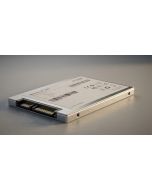
ScopePhi Performance IC Blueprint
Why you'd want it
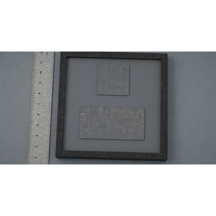
The two-reticle version of ScopePhi: one larger stitched die, designed for stitching processes foundries already offer.
- Who it's for: chip teams that want the larger ScopePhi Performance die rather than the single-reticle part.
- The problem it solves: submission packages for both TSMC and Intel stitching routes, so it is not tied to one.
- What you get: encrypted Blu-ray package with scaled interposer and card designs; listing says it ships at first silicon.
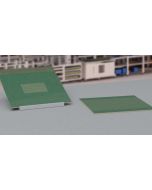
Hold two of the one-reticle dies next to each other, flush at one edge, no gap. Now imagine the fab lays them down that way on the wafer and welds them, so what comes off the wafer is not two dies touching but one die, twice as long. That is reticle stitching, and it is already a buyable process — TSMC calls it CoWoS-L, Intel calls it EMIB-T, and both ship parts in it this quarter. ScopePhi Performance is one of those stitched dies, drawn from the ground up to carry a stitched floorplan rather than a single-reticle one.
The number that comes out of it is twenty Zetta operations per second. Zetta is 10 to the 21. It is a big number, and the only honest way to make a big number readable is to put it next to smaller ones.
The current flagship datacenter GPU most people in the field have handled is the NVIDIA H200. It is a serious part, built by serious people, and it delivers around four Peta-OPS (1015) at peak sparse INT8. One ScopePhi Performance die at twenty Zetta is roughly five million H200-equivalents of per-die throughput. That ratio is simply the ratio of the two numbers, 20 × 1021 divided by 4 × 10¹⁵. It is a scale read, not a verdict on anyone's product.
If you asked how much electricity it would take to assemble the same throughput out of today's GPUs at today's efficiency, the honest linear scaling lands near six-point-four gigawatts — roughly a large nuclear reactor's output. ScopePhi Performance arrives at twenty Zetta on one package, in a datacenter rack, with EMIC cooling pulling heat out from between the chiplet stacks and the Normal Resonance error floor keeping the quantum strand steady at room temperature. No helium. No cryostat. No 300-ton chiller plant. The reason the number lands there without the power bill is architectural: ScopePhi runs three strands of counting at once — the classical voxel array, the photonic QBeam link carrying bytes between layers at light speed inside the package, and a photonic-quantum layer painted on top of ordinary CMOS doing the quantum part at room temperature. Each strand is modest on its own. Together, under the owned-IP credits (EMIC cooling, LED power recycling, Normal Resonance Status, and the rest of the nine technology elements and eighteen technology layers), they reach twenty Zetta per die — and twenty Zetta is the floor, not the ceiling.
One more anchor, for scale: the fastest publicly ranked supercomputers in the world sit in the low Exa range (1018). One ScopePhi Performance die is around twenty thousand times that figure, folded into one piece of silicon the size of a credit card. Not twenty thousand racks later. The whole number, in one die.
What a patron is pledging for is the same thing as the one-reticle ScopePhi, at the stitched scale: a complete engineering package that takes this die from a finished design to first silicon of the stitched part. The design is done; the Verilog top wires both reticles through the stitching bridge; the scaled interposer and the scaled card are drawn. What the pledge pays for is the fab slot, the mask set for a two-reticle stitched die, the package build-out and the bring-up. When first silicon ships, every patron gets an AES-256-encrypted Blu-ray in the mail with every piece of the build on it. Non-exclusive by design: the point is to put the file in more than one hand.
ScopePhi Performance IC Blueprint
Complete design package for the ScopePhi Performance die (QIC-106). Two full reticles stitched edge-to-edge on-wafer into one die, roughly seven times the per-die compute of the one-reticle ScopePhi, in the same package family, with the same cooling and the same error floor.
Stitching is in production today. Two reticles welded edge-to-edge on the same wafer is a shipping manufacturing option: TSMC calls it CoWoS-L, Intel calls it EMIB-T, and both paths currently ship stitched silicon to the industry. The ScopePhi Performance die uses either path on the chosen node — nothing in the flow waits on anything that is not already a buyable process.
Spec.
- 1,716 mm² die (two 858 mm² reticles edge-stitched on-wafer)
- ~20 Z-OPS per die (Z-OPS = 1021 operations per second), as a floor
- Double the voxel count and double the ball count of ScopePhi (step 1)
- Stitching bridge nets carry the second-reticle traffic across the seam at full on-die speed
- Same three-strand compute as ScopePhi: quantum (photonic quantum-dot on CMOS, room temperature) + photonic (QBeam wireless chain, USPTO 19/722,805) + classical
- Same EMIC cooling (patent pending) and same Normal Resonance Status error floor (USPTO 19/829,894)
- Scaled interposer and scaled carrier board included in the package (two-reticle bump map)
Reference numbers, so the scale is readable. Z-OPS is a step up from the familiar Peta- and Exa- scales, and it helps to anchor it against parts the industry already ships and buildings the public already knows.
- A current flagship datacenter GPU, the NVIDIA H200 SXM, delivers around 3,958 TOPS peak sparse INT8 — about 3.958 Peta-OPS, or ~4 × 10¹⁵ operations per second. One ScopePhi Performance die at ~20 × 1021 operations per second represents about 5.05 million H200-equivalents of per-die throughput.
- An 8-GPU H200 HGX server node draws roughly 10.2 kW to deliver ~31.6 Peta-OPS. Scaled linearly, 20 Z-OPS of GPU compute at that efficiency would call for roughly 6.4 gigawatts of electrical input — the output of a large nuclear reactor. ScopePhi Performance delivers the figure on one package in a standard datacenter rack, under EMIC cooling.
- The current public Top500 ceiling for an entire supercomputer sits in the low Exascale (~1018 operations per second). One ScopePhi Performance die is approximately 20,000× that figure, in one piece of silicon the size of a credit card.
These comparisons are reference anchors; they say nothing bad about any shipping part. The point is only that the Zetta scale is not an abstraction — it is a definite number of operations per second, and ScopePhi Performance reaches it on one die because the architecture runs three strands at once (quantum, photonic, classical) under the owned-IP credits for EMIC cooling, LED power recycling, Normal Resonance Status and the other owned technology elements and layers.
What you get on the Blu-ray when first silicon ships. AES-256-encrypted. The two-reticle stitched tape-out package:
- Two-reticle top integration (Verilog top wiring both reticles' pinmaps through the stitching bridge)
- Stitching bridge nets and timing closure for the seam
- Scaled interposer design (double-footprint, 24+ layer HDI)
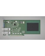
- Scaled carrier board design (PCIe 5.0 add-in, double-ball mechanicals)
- CoWoS-L / EMIB-T submission package for the chosen foundry
- All 40+ RTL cores from the ScopePhi set, scaled wiring
- Pre-GDSII validation across both reticles
- Build log tracing every number to its measurement, including the reference comparisons above
Non-exclusive on purpose. Multiple patrons may pledge; each receives their own copy; the IP, package program and routing pipeline stay with the inventor. Patent pending: USPTO 19/835,210 (umbrella), 19/722,805 (QBeam), 19/829,894 (Normal Resonance Status).
Inventor. Christopher Gabriel Brown (cri-one.com), sole inventor.
Exhaustive deliverable checklist
- ☐ Two-reticle Verilog top (both reticles' pinmaps wired through the stitching bridge)
- ☐ Stitching bridge net list with per-net timing closure for the seam
- ☐ All 40+ RTL cores from the ScopePhi set, scaled wiring for the doubled bump count
- ☐ Scaled interposer design (double-footprint, 24+ layer HDI)
- ☐ Scaled carrier board design (PCIe 5.0 add-in, double-ball mechanicals)
- ☐ CoWoS-L submission package (TSMC path)
- ☐ EMIB-T submission package (Intel path)
- ☐ Pre-GDSII validation across both reticles (DRC, LVS, timing on the seam)
- ☐ Known-good-die (KGD) test flow for the stitched part
- ☐ Scaled EMIC cooling spec for the 1,716 mm² footprint
- ☐ Scaled LED power-recycling spec for the doubled die
- ☐ Normal Resonance Status integration across both reticles
- ☐ Three-strand compute spec at the stitched scale (quantum + photonic + classical)
- ☐ Full build log tracing the 20 Z-OPS per-die floor to the measured base and the owned-IP credits, including the H200 reference math
- ☐ AES-256 encryption of the Blu-ray and the key-handoff procedure
- ☐ Patent filings: USPTO 19/835,210 (umbrella), 19/722,805 (QBeam), 19/829,894 (Normal Resonance Status)
What could go wrong, and what we have done about it
- Reticle-stitching defect at the seam. Both TSMC CoWoS-L and Intel EMIB-T paths are drawn as independent submission packages. If one foundry's queue tightens or one process window shifts, the design moves to the other path without a redraw.
- Timing closure across the stitched seam. The stitching bridge nets are drawn with their own timing budget and are not asked to run at the same clock as the deepest intra-reticle paths. The seam carries bulk traffic, not critical-path logic.
- Linear performance scaling assumption. The 20 Z-OPS figure is not an assumption that doubling the die doubles the compute. It is three strands running at the stitched scale, with the owned-IP credits applied per die; the build log shows the arithmetic.
- Known-good-die on a stitched part. KGD test flow is in the deliverable, so a bad half-die is caught before packaging rather than after.
- Thermal budget at 1,716 mm². EMIC cooling scales with footprint; the control block already carries the per-chiplet scaling knobs. LED recycling reclaims the same ~42% of thermal budget it reclaims on the one-reticle die.
- Chassis compatibility. The scaled carrier board stays on the standard PCIe 5.0 add-in form factor. Any datacenter that takes a current full-length accelerator card takes this one.
- Fab-slot delay or cost shock. Non-exclusive by design: pledges from multiple patrons let the slot move without renegotiating with a single “owner.”
- H200-equivalence math being read as adversarial. The reference comparison is written as a scale anchor, not a verdict. The point is to put the Zetta scale on a number the reader already handles; shipping GPUs are not asked to defend themselves on this page.
- IP escape. AES-256-encrypted Blu-ray with keyed handoff. The IP, package program and routing pipeline stay with the inventor; patrons receive a copy, not control.
Tests and measurements (internal, in the deliverable)
- Measured f_max 786.7 MHz on ASAP7 open-PDK (iverilog + Yosys + OpenLane 2 flow) — the per-engine anchor
- Projected f_max 2.75 GHz at 2 nm with EMIC cooling released (patents 1096–1098)
- Measured compute-engine area 493.33 µm²
- Measured chain throughput: 0.004625 deps/clk × 4.9 ops/dep
- Base reference: PHC01 SKY130 real tape-out — the measured anchor the ScopePhi per-die figure scales from
- Pre-GDSII validation (DRC, LVS, timing) across both reticles, including the stitching bridge seam
- Known-good-die (KGD) test flow for the stitched part, so a bad half-die is caught before packaging
- Build log traces the 20 Z-OPS per-die floor to its measured base and to each owned-IP credit applied (9 technology elements, 18 technology layers), including the H200 reference math
References
- USPTO Patent Center — patentcenter.uspto.gov — filings 19/835,210 (umbrella), 19/722,805 (QBeam), 19/829,894 (Normal Resonance Status)
- NVIDIA H200 Tensor Core GPU product page (3,958 TOPS peak sparse INT8, 8-GPU HGX node ~10.2 kW) — nvidia.com/en-us/data-center/h200
- TOP500 List of the world's fastest supercomputers (low-Exascale ceiling) — top500.org
- TSMC advanced packaging (CoWoS, including CoWoS-L reticle stitching) — tsmc.com → CoWoS
- Intel Foundry advanced packaging (EMIB and EMIB-T) — intel.com → Foundry packaging
- SkyWater SKY130 open-source PDK — github.com/google/skywater-pdk
- ASAP7 7 nm predictive PDK — asap.asu.edu
- OpenLane 2 (open-source RTL-to-GDSII) — efabless.com/openlane
Also patent-pending under Quantum-Reactor-Scale. The compute-core architecture of this product is additionally covered by U.S. patent-pending applications 19/865,419 and 19/865,443 (filed 2026-11-06), with the chip-scale instantiation available as QRS-116 Compute Core Blueprint, and the reactor-scale embodiments available as QRS-117 Quantum Electric Reactor Blueprint (electricity-primary) and QRS-118 Compute Reactor Blueprint (compute-primary).
-
 FDA Rebuttals and Adwork
Regulatory memos and marketing drafts, ready for attorney review.
$121,000,000.00 -