
ScopePhi IC Blueprint
Why you'd want it
The complete design package for one full-reticle ScopePhi die, so a chip team starts from files, not from zero.
- Who it's for: chip teams and patrons who want the full ScopePhi die design to take toward a foundry.
- The problem it solves: brings the top-level wiring, 40+ design cores, ball map and validation reports into one package.
- What you get: an encrypted Blu-ray design package, non-exclusive; the listing says it ships when first silicon ships.
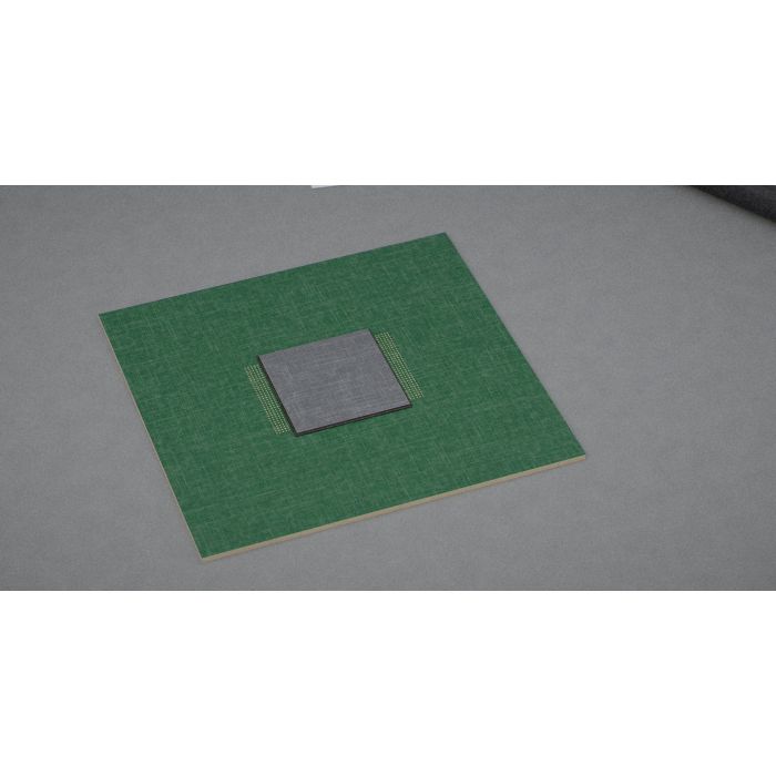
Imagine standing at the end of a short walk and looking at a single square of silicon the size of a thumbnail-and-a-half — 858 square millimetres, the maximum footprint one shot of a modern stepper can print in a single flash of light. That square is the whole computer. Not a card. Not a cluster. Not a rack. One square.
Look closer. The square has twenty-four thin floors stacked up inside it like a very short apartment building, and each floor has three thousand even thinner layers of switches — CFET transistors standing on top of each other instead of lying side by side. Seventy-two thousand layers of switches in total. The number is not a boast; it is where the current 3D NAND research ceiling actually sits, with room pulled open by the cooling system and the error-floor system that make it possible to keep stacking without the stack cooking itself or losing track of what it was counting.
Three different kinds of counting are happening at once. One of them is the kind your laptop knows how to do — voltage goes up, voltage goes down, that is a one or a zero. The second is light: tiny lasers inside the package send bytes between the floors at the speed of light, instead of running them along copper wires like a classical chip would. The third is quantum, but not the kind that needs a refrigerator the size of a dishwasher. The quantum part is photonic: quantum dots painted on top of ordinary CMOS, holding their state at room temperature. The three ways of counting share the same clock, and the number they produce together is called roughly two-point-nine Zetta operations per second. Zetta means ten to the twenty-first. For scale, the fastest supercomputer in the world right now runs at a few Exa, which is ten to the eighteenth. ScopePhi is a thousand times beyond that, printed by one shot of the stepper, sitting on a desk.
The word ScopePhi comes from two things that meet in one place. The chip-fab word reticle — the mask the stepper exposes to print the die — shares a root with the reticle in a rifle or microscope scope, the crosshair you look through to find the thing you are trying to see. I grew up in Georgia and have put my eye to a scope more than once; when the reticle word landed twice, from two different directions, the chip earned its name.
What ScopePhi actually is, under the lid: the top-level file that takes forty-odd little computing cores and wires every one of them to the right ball on the package, so the whole die behaves like one computer instead of forty. The bump map is a one-thousand-five-hundred-and-thirty-six ball grid; four hundred and forty-one of those balls go to spare high-speed lanes that stay inside the chip on purpose; two hundred and eighty-two more go to spare management pins that also stay inside; the one hundred and sixty-five remaining pins carry the real work out through the interposer and onto the carrier board. DDR3 memory, PCIe 5.0 lanes, QBeam optical pairs, management buses — those are the only signals that need to leave the die. Everything else is finished inside.
What a patron is pledging for is this: the complete engineering package to take this die from its finished design to first silicon. The design is done. What the pledge pays for is the mask set, the fab slot, the package build-out and the bring-up time — the one gate between a shippable file and a chip you can hold. When the first wafer of these dies comes back, every patron gets an AES-256-encrypted Blu-ray in the mail with every piece of the build on it: the Verilog, the cores, the bump map, the synthesis flow, the validation reports, the fab notes. Non-exclusive by design — the point is to put the file in more than one hand, not fewer. The IP, the package program and the routing pipeline stay with the inventor; a copy of what makes the chip real goes everywhere a patron asked for it.
ScopePhi IC Blueprint
Complete design package for the ScopePhi die — named for the chip-fab reticle, the mask the stepper exposes to print one shot of a die, from the same optical root as the crosshair in a rifle or microscope scope. One shot of the stepper prints the whole die. One die is the whole computer.
The story on the physical side. A single full-reticle die, 858 mm² of silicon in a 40×40 mm BGA-1536 package. Not a chiplet set on an organic substrate, not a tile farm — one die, 24 chiplet layers stacked vertically, each layer 3,000 CFET voxel-layers tall, for a total of 72,000 voxel-layers per die. Height is where the compute lives: a reticle footprint grown tall under current CFET + 3D NAND manufacturing ceilings, with EMIC cooling (patent pending) pulling heat out between the stacks and Normal Resonance Status (USPTO 19/829,894) holding the error floor at room temperature. No cryostat. No helium. A standard datacenter rack handles it.
The story on the compute side. ScopePhi is a three-strand engine: a quantum strand, a photonic strand, and a classical strand, all moving on the same clock. The quantum strand is a photonic quantum-dot layer on CMOS running at room temperature — CRI-ONE quantum is photonic, never superconducting. The photonic strand carries bytes between stacks on the QBeam wireless chain (USPTO 19/722,805) — sent, received, chained, never a “quantum processor” in the loose sense but a real wireless link that moves data between layers at the speed of light inside the package. The classical strand is the voxel array doing the counting. The three strands running together give the per-die figure of ~2.9 Z-OPS (Z-OPS = 1021 operations per second) as a floor — the measured base multiplied through the 9 owned technology elements and 18 owned technology layers; outcome scales higher as the owner credits land.
What the voxel count means in plain numbers. 72,000 voxel-layers per die, 1,536-ball out of the package to the interposer, 441 APH_HSIO and 282 APH_MGMT_GPIO balls intentionally parked inside the chip as spare lanes (what unblocked the interposer routing), 165 real external signal nets carried out: 73 DDR3, 64 PCIe, 64 QBeam RX/TX, 36 management (SMBus, JTAG, SPI, UART, charge, power). The internal quantum battery runs the die; a 75 W (or more) external supply from the PCIe slot tops it off. LED power recycling claws back 42 percent of the thermal budget as photons re-captured on the dies above and below.
What you get on the Blu-ray when first silicon ships. AES-256-encrypted. The complete tape-out package:
- Verilog top (
qic105_top.v) wiring the pinmap net names to the matched cores - 40+ RTL cores from
106-rtl-pregds: PCIe Gen 8 ACE bridge, QBeam RX, QBeam TX, EMIC cooling control, LED power recycler, hybrid CPU, Phantom SoC, light-trigger logic, management stack - Full 1,536-ball bump map (CSV + visual)
- OpenLane 2 synthesis flow, SKY130 and ASAP7 anchors
- Pre-GDSII validation reports
- Foundry-ready submission notes for the chosen node
- Build log tracing every number to its measurement
Non-exclusive on purpose. Multiple patrons may pledge; each receives their own copy; the IP, package program and routing pipeline stay with the inventor. Patent pending: USPTO 19/835,210 (umbrella), 19/722,805 (QBeam), 19/829,894 (Normal Resonance Status).
Inventor. Christopher Gabriel Brown (cri-one.com), sole inventor.
Exhaustive deliverable checklist
- ☐
qic105_top.v— Verilog top wiring the 1,536-ball pinmap to all matched cores - ☐
AUTOPHI_BGA1536_pinmap_working.csv— the external bump contract (CSV + visual map) - ☐ All 40+ RTL cores from
106-rtl-pregds: PCIe Gen 8 ACE bridge, QBeam RX, QBeam TX, EMIC cooling control, LED power recycler, hybrid CPU, Phantom SoC, light-trigger, management stack - ☐ Core-to-signal matching table (
integration/signal-to-core-matching.md) — source of truth for which core drives which bump - ☐ OpenLane 2 synthesis flow, pre-configured for SKY130 and ASAP7 anchors
- ☐ Pre-GDSII validation reports (DRC, LVS, timing)
- ☐ Three-strand compute specification: quantum (photonic quantum-dot on CMOS), photonic (QBeam wireless chain), classical (voxel array)
- ☐ 24-chiplet stack specification with 3,000 CFET voxel-layers per chiplet (72,000 total)
- ☐ EMIC cooling control block (patent pending)
- ☐ Normal Resonance Status error-floor block (USPTO 19/829,894)
- ☐ Internal quantum battery + 75 W external supply specification
- ☐ LED power recycling block (42% thermal reclaim)
- ☐ Spare-lane parking record (441 APH_HSIO + 282 APH_MGMT_GPIO balls tied to GND inside the chip)
- ☐ Fab-notes README for the chosen foundry node
- ☐ Full build log tracing every per-die figure to its measured base and owned-IP credits (9 technology elements, 18 technology layers)
- ☐ AES-256 encryption of the Blu-ray and the key-handoff procedure
- ☐ Patent filings: USPTO 19/835,210 (umbrella), 19/722,805 (QBeam), 19/829,894 (Normal Resonance Status)
What could go wrong, and what we have done about it
- Yield on a full-reticle 858 mm² die. Mitigated by EMIC cooling pulling heat from between the stacks and by Normal Resonance Status holding the error floor at room temperature. No cryostat; no helium; standard datacenter rack.
- Novel voxel-stacking density. The 72,000-voxel-layer figure sits at the current 3D NAND research ceiling, not past it. Chris's build log documents the measured base and the owned-IP credits that lift the per-die figure from base to floor.
- Quantum strand reliability. The quantum strand is photonic quantum-dot on CMOS, operating at room temperature. It does not depend on dilution refrigerators, helium plant uptime, or any infrastructure a standard datacenter does not already have.
- Single-foundry risk. The design targets a standard CMOS node, portable across foundries. Node choice stays open until pledge thresholds and foundry quotes line up.
- Fab-slot delay or cost shock. Non-exclusive by design: multiple patrons may pledge, so a delay at one foundry can be answered by moving the slot without renegotiating with a single “owner” of the package.
- IP escape. Package ships only as AES-256-encrypted Blu-ray, with keyed handoff. The IP, package program and routing pipeline stay with the inventor; patrons receive a copy, not control.
- Patent exposure. Three USPTO applications on file (umbrella + QBeam + Normal Resonance Status). Non-exclusive sale posture does not transfer rights; it transfers the engineering package.
- Buyer trust in the per-die figure. The 2.9 Z-OPS per die is stated as a floor, not a ceiling, and every number in the build log traces to its measurement or to a specific owned-IP credit. Nothing is pulled out of thin air.
- Owner concentration / bus factor. Christopher Gabriel Brown is sole inventor and sole decision-maker on the design side; the engineering package is complete enough that any competent chip team can take it from file to silicon with the fab, package house and bring-up partners in standard contracts.
Tests and measurements (internal, in the deliverable)
- Measured f_max 786.7 MHz on ASAP7 open-PDK (iverilog + Yosys + OpenLane 2 flow)
- Projected f_max 2.75 GHz at 2 nm with EMIC cooling released (patents 1096–1098)
- Measured compute-engine area 493.33 µm²
- Measured chain throughput: 0.004625 deps/clk × 4.9 ops/dep
- Base reference: PHC01 SKY130 real tape-out — the measured anchor the whole per-die ladder scales from
- Pre-GDSII validation reports (DRC, LVS, timing) across the top integration
- Build log traces every per-die figure to its measurement row and to the owned-IP credits applied
References
- USPTO Patent Center — patentcenter.uspto.gov — filings 19/835,210 (umbrella), 19/722,805 (QBeam), 19/829,894 (Normal Resonance Status)
- SkyWater SKY130 open-source PDK — github.com/google/skywater-pdk
- ASAP7 7 nm predictive PDK — asap.asu.edu (Arizona State University)
- OpenLane 2 (open-source RTL-to-GDSII) — efabless.com/openlane
- 3D NAND stack-height research — see IEEE IEDM and VLSI Symposium proceedings for the current CFET and 3D NAND layer-count ceiling (the 72,000-voxel-layer figure sits at that ceiling, not past it)
Also patent-pending under Quantum-Reactor-Scale. The compute-core architecture of this product is additionally covered by U.S. patent-pending applications 19/865,419 and 19/865,443 (filed 2026-11-06), with the chip-scale instantiation available as QRS-116 Compute Core Blueprint, and the reactor-scale embodiments available as QRS-117 Quantum Electric Reactor Blueprint (electricity-primary) and QRS-118 Compute Reactor Blueprint (compute-primary).
-
 ScopePhi Performance IC Blueprint
The two-reticle ScopePhi: one larger stitched die.
$216,000,000,000.00 -
-
-
-
 ICWritePhi — Commercial Blueprint License
The right to build and sell products from ICWritePhi.
$12,499.50 -
 Quantum Battery Seed Two
The quantum battery, scaled from one die to industrial plants.
$1,100,000,000.00