
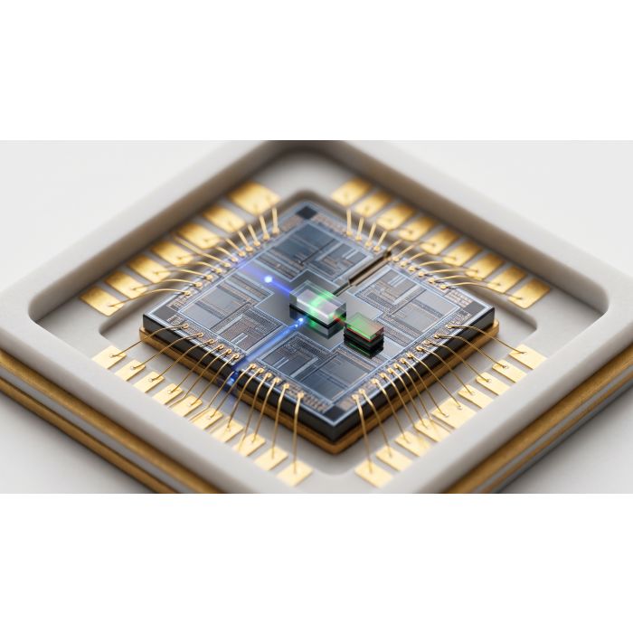
QRS-116 Compute Core Blueprint
Think of a computer chip the size of a fingernail that does more arithmetic in a second than a modern data center does in a month, runs on a sliver of safe nuclear fuel for twenty-five years without being plugged in, and talks to its neighbors with light instead of wires. Inside the chip, blue laser light pumps a tiny crystal that splits each photon into many; those photons ring back and forth between two mirrors, gaining strength the way a child on a swing gains height; a smaller crystal translates the ringing light into measurable colors that the chip's own CMOS brain reads as numbers. A dusting of nickel-63 (the same isotope used in smoke-detector-grade beta sources) and carbon-14 provides a trickle of electricity around the clock, so the chip doesn't need a wall outlet. The blueprint spells out the mirrors, the crystals, the catalyst layers, the CMOS brain, the radiolucent isotope source, and how to make them in a standard semiconductor fab. One license covers every scale, from this chip to the reactor built around it.
What this is. An engineering blueprint and reduction-to-practice data set for a multi-catalyst coupling-matrix compute die, covered by claim 1 of U.S. patent-pending application 19/865,419 (filed 2026-11-06). The die integrates five elements on one substrate: a Fabry-Perot resonant optical cavity, three catalyst input stages at mutually distinct wave bands (optical / microwave / radioluminescent-nuclear baseline), a nonlinear medium performing four-wave mixing, a CMOS digital controller measuring a loop-gain tensor with at least one scalar element per catalyst pathway, and a multi-chromophore crystal readout stage.
What is in the data set. Full Verilog register-transfer-level source for the controller: 10,330 cells baseline (Project 05 quantum battery, verified 2026-11-05) plus 31,601 additional cells for the catalyst-input stages, cavity controller, multi-chromophore crystal readout, reservoir trainer, and loop-gain-matrix storage block (verified 2026-11-06). Combined 41,931 cells on SKY130 at typical-typical / 25°C / 1.80V. Synthesis report included. Register-map specification for the APB and AXI4-Lite interfaces. Q8.24 fixed-point loop-gain tensor storage with single-cycle access and a trace-exceeds-unity first-law alarm bit. Reservoir-trainer with 32-tap multiply-accumulate and least-mean-squares weight updates. Analog-front-end specification for the piezoelectric mirror driver, interferometric phase sensor, and multi-channel analog-to-digital converter.
What it enables. Programmable hardware multiplication at the speed of light. Compute output on top of exergy transport. A measurement architecture that no known photonic-compute prior art implements, because every prior art scales to one pump source.
Priority. The inventor's 2017 dated disclosures of invention #957 through #960 (the "light tunnel of amped reflected focused light; oscillating and inverted re-emission") anchor the bidirectional resonant cavity architecture nine years ahead of post-2017 citations.
Scales. This blueprint is the subcombination that scales from chip voxel (~1 mm²) through handheld, building (1-45 m², kW-MW), tower (26,624 dies per Project 114's stacking), and reactor facility (see QRS-117). The same controller IP is inherited at every scale.
License posture. Non-exclusive. Fabrication partnership welcome. Contact christopher\@cri-one.com. U.S. patent-pending, application 19/865,419.