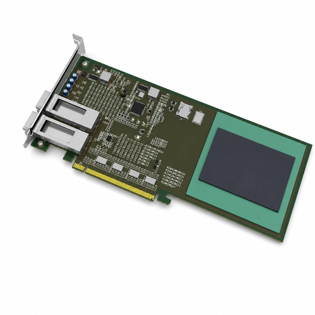
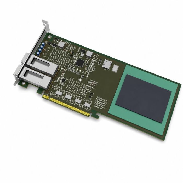
35-autophi-quantum-pcie5

$99,999,999.00
In stock
SKU
2064
Asset valuation: $25,000,000,000. Inventor: Christopher Gabriel Brown Website: CRI-ONE.COM Date: March 31, 2026 Last edited: 2026-04-24 Complete engineering blueprint for a PCIe 5.0 x16 accelerator card built around the AutoPhi Quantum Battery System IC. 34 I/O bracket variants, custom autorouter wi

Valuation

Generous asset valuation: $25,000,000,000. The listed price is the platform maximum; acquisition at valuation is handled by direct enquiry.

Project 35: AutoPhi Quantum PCIe 5.0 Accelerator Card

Project 35: AutoPhi Quantum PCIe 5.0 Accelerator Card

Inventor: Christopher Gabriel Brown

Website: CRI-ONE.COM

Date: March 31, 2026

Last edited: 2026-04-24

Overview

Complete engineering blueprint for a PCIe 5.0 x16 accelerator card built around the

AutoPhi Quantum Battery System IC. 34 I/O bracket variants, custom autorouter with

RAG knowledge base, and KiCad plugin.

 PCIe x16 Edge     5x DS80PCI810     AutoPhi BGA-256     4x DDR3 FBGA-96
  Connector J1  -->  Retimers     -->   Main IC U1    -->  Memory U63-U66
  (164 pins)       (U2-U5, U8)       (22x22mm)          (11x15mm each)

Current Status

Board 01 (qsfp28-optical): Routing in progress with fixed Edge.Cuts boundary enforcement.

See STATUS.md for detailed metrics.

34 Board Variants

All share the same core PCB -- differ only in I/O bracket connector (J2/J3):

Full details: blueprints/VARIANTS.md

Project Structure

autophi_engine/        Core Python library (7,248 lines)
  rag/                 RAG knowledge base (50+ citations, 18 net classes)
  layout/              Board geometry (outline, placement, routing, vias)
  output/              File export (KiCad PCB, Gerber, SVG)
  verify/              Design rule checking

blueprints/            Pipeline scripts (14,000+ lines)
  auto_route.py        A* maze router (core, 1,749 lines)
  drc_check.py         Post-route DRC verification
  render_board_svg.py  SVG preview renderer
  boards/              34 board variant directories
  route_cache/         Cached routing paths

KiCad Plugin           5 action plugins for KiCad 10.0
  Route, Via Cascade, DRC Check, Smart Place, Unroute

Quick Start

# Route board 01
python blueprints/auto_route.py "blueprints/boards/01-qsfp28-optical/autophi-pcie5-qsfp28-optical.kicad_pcb" \
  --exclude-refs J2,J3,J4 --grid 0.12 --timeout 15

# DRC check
python blueprints/drc_check.py "blueprints/boards/01-qsfp28-optical/autophi-pcie5-qsfp28-optical.kicad_pcb"

# Render SVG preview
python blueprints/render_board_svg.py "blueprints/boards/01-qsfp28-optical/autophi-pcie5-qsfp28-optical.kicad_pcb"

# Build all 34 variants
python blueprints/build_all.py

Key Features

  • PCIe 5.0 x16 interface (128 GB/s aggregate bandwidth)
  • AutoPhi Quantum Battery System IC (BGA-256, 1.0mm pitch)
  • 5x DS80PCI810 retimers for signal integrity
  • 4x DDR3 SDRAM (FBGA-96)
  • 10-layer PCB stackup (5 signal + 3 GND + 2 power)
  • Custom A* maze router with 50+ RAG citations
  • All traces and components stay within board boundaries

Documentation Index

Patent Coverage

  • 18/370,908 -- Quantum Battery System
  • 19/403,339 -- Optical Quantum Battery
  • 3561/2876 -- Light Trigger Semiconductor
  • 1026 -- Battery + Generator + Recycle
  • 1096-1098 -- EM Field Control
  • 1105 -- Wind Recycle Generator
  • 3559 -- Staircase Mirror Chip

Contact

Christopher Gabriel Brown

Email: chris@cri-one.com

Website: https://cri-one.com

AutoPhi Quantum PCIe 5.0 -- System Architecture

AutoPhi Quantum PCIe 5.0 -- System Architecture

> Christopher Gabriel Brown | CRI-ONE.COM | March 2026

Hardware Architecture

The AutoPhi Quantum PCIe 5.0 is a full-length PCIe 5.0 x16 accelerator card based on the

Texas Instruments TIDA-00423 reference design. The board carries ~350 components across

a 10-layer PCB.

Block Diagram

                        +-----------+
                        | PCIe x16  |  J1 (164 pins, 1mm pitch)
                        | Edge Conn |  A-side B.Cu / B-side F.Cu
                        +-----+-----+
                              |
              PCIe Gen5 x16 differential pairs (32 GT/s, 85 ohm)
              16 TX lanes + 16 RX lanes + REFCLK + sideband
                              |
         +--------------------+--------------------+
         |          |         |         |          |
    +----+----+ +---+---+ +--+---+ +---+---+ +----+----+
    | DS80    | | DS80  | | DS80 | | DS80  | | DS80    |
    | PCI810  | | PCI810| | PCI810| | PCI810| | PCI810  |
    | U2      | | U3    | | U4   | | U5    | | U8      |
    | Retimer | | Retmr | | Retmr| | Retmr | | Retimer |
    +----+----+ +---+---+ +--+---+ +---+---+ +----+----+
         |          |         |         |          |
         +----+-----+---------+---------+-----+----+
              |                                |
         +----+--------------------------------+----+
         |        AutoPhi Quantum BGA-256           |
         |              U1 (Main IC)                |
         |   22x22mm body, 1.0mm pitch, 16 rows     |
         |   PCIe MAC + DDR3 controller + quantum   |
         |   execution unit + thermal management    |
         +---+----+----+----+----+----+----+---+----+
             |    |    |    |    |    |    |   |
            DDR  DDR  DDR  DDR  SPI  I2C JTAG UART
            DQ   ADDR CLK  CTRL
             |    |    |    |
        +----+  +-+  +-+  +-+
        |       |    |    |
   +----+----+ ++---++ +--+--+  +-------+
   | DDR3    | | DDR3 | | DDR3| | DDR3  |
   | FBGA-96 | | FBGA | | FBGA| | FBGA  |
   | U63     | | U64  | | U65 | | U66   |
   +---------+ +------+ +-----+ +-------+

   +--------+   +--------+
   | I/O    |   | Power  |
   | Bracket|   | Supply |
   | J2/J3  |   | U6/U7  |
   +--------+   +--------+

Key Components

10-Layer PCB Stackup

Target fabrication: JLCPCB, 1.6mm thickness, Megtron 6 dielectric.

Routable signal layers (used by auto_route.py): F.Cu, In2.Cu, In4.Cu, In6.Cu, B.Cu (5 layers).

Impedance targets: 85 ohm differential (PCIe Gen3+), 50 ohm single-ended, +/-10% tolerance.

Software Architecture

Three codebases work together:

+---------------------------+     +---------------------------+
|    autophi_engine/        |     |    KiCad Plugin           |
|    (Python library)       |     |    (wxPython UI)          |
|                           |     |                           |
|  rag/  -- knowledge base  |     |  Route, Via Cascade,      |
|  layout/ -- geometry      |<----|  DRC Check, Smart Place,  |
|  output/ -- file export   |     |  Unroute All              |
|  verify/ -- DRC           |     +---------------------------+
+------------+--------------+
             |
             | imported by
             v
+---------------------------+
|    blueprints/            |
|    (pipeline scripts)     |
|                           |
|  auto_route.py   -- A* maze router (core)
|  drc_check.py    -- post-route DRC
|  render_board_svg.py -- SVG preview
|  fork_ti_board.py    -- TI -> 34 variants
|  build_all.py        -- master pipeline
|  ...30+ more scripts
+---------------------------+
             |
             | reads/writes
             v
+---------------------------+
|  blueprints/boards/       |
|  34 board variants        |
|  .kicad_pcb files         |
|  preview SVGs             |
|  route cache JSON         |
+---------------------------+

autophi_engine Package

blueprints Pipeline

Net Classification System

The RAG assigns every net to one of 18 classes. The router uses class membership to

determine trace width, clearance, via cost, priority order, and preferred layer.

RAG Knowledge Base

The RAG (Retrieval-Augmented Generation) knowledge base grounds every routing decision

in cited sources. The router logs which citations it consulted at runtime.

50+ citations from:

  • PCB design guides: Sierra Circuits, PCBway, Altium, AllPCB, FS-PCBA [1-18]
  • Textbooks: Johnson & Graham "High-Speed Digital Design" [19], Zhang/Krooswyk/Ou [20]
  • JLCPCB fabrication specs: 15 separate capability documents [21-31]
  • TI TIDA-00423 reference design art film [32]
  • Wikipedia: octilinear routing, EDA routing [33, 14]
  • AutoPhi internal discoveries: DRC-safe mechanism [47]
  • Local textbook PDFs: geometry, calculus, PCB fabrication [48-50]

15+ configuration dicts in autophi_engine/rag/routing.py:

CITATIONS, NET_CLASS_RULES, NET_CLASSES, A_STAR, VIA_SPAN_COST,

LAYER_POLICY, BGA_FANOUT, RETURN_PATH, FABRICATION, JLCPCB,

ROUTING_ORDER, KEEPOUT, ANY_ANGLE, DRC_SAFE, TI_STYLE

Fabrication Constraints (JLCPCB 6+ Layer)

Related Documents

  • STATUS.md -- Current routing metrics and DRC results
  • blueprints/README.md -- Pipeline script guide
  • autophi_engine/README.md -- Engine API reference
  • blueprints/MANUFACTURING.md -- Fab specifications
  • blueprints/KICAD_PLUGIN.md -- KiCad action plugins

35 - Autophi Quantum Pcie5

35 - Autophi Quantum Pcie5

> Internal playbook -- not for public eyes.

> Last scaffolded: 2026-05-11

1. Identity

2. One-liner

> Complete engineering blueprint for a PCIe 5.0 x16 accelerator card built around the AutoPhi Quantum Battery System IC. 34 I/O bracket variants, custom autorouter with RAG knowledge base, and KiCad plugin.

*(Edit this once. It becomes the single sentence you reuse in replies,

on the catalog page, and at the top of any future write-up.)*

3. What's actually in the folder

  • .claude/ (1 entries)
  • _ti_rag_render/ (7 entries)
  • Apples/ (21 entries)
  • autophi_engine/ (8 entries)
  • blueprints/ (82 entries)
  • handoffs/ (1 entries)
  • kicad-footprints-master/ (1 entries)
  • output/ (4 entries)
  • part/ (8 entries)
  • sales-pitches/ (3 entries)
  • ARCHITECTURE.md
  • CHANGELOG.md
  • CONTACT_INFO.txt
  • CONTRIBUTING.md
  • MANIFEST.json
  • PLAYBOOK.md
  • README.md
  • SESSION_VICTORY_20260413.md
  • STATUS.md
  • tidrd10.pdf
  • tidrd12.pdf
  • tidrd13 (1).pdf
  • tidrd13.pdf
  • tidrd14.zip

4. README at a glance

Top sections found in README.md:

  • Overview
  • Current Status
  • 34 Board Variants
  • Project Structure
  • Quick Start
  • Key Features
  • Documentation Index
  • Patent Coverage

(Full text: D:\special\35-autophi-quantum-pcie5\README.md)

5. Hook lines (pick the one that fits the reader)

  • (default) Complete engineering blueprint for a PCIe 5.0 x16 accelerator card built around the AutoPhi Quantum Battery System IC. 34 I/O bracket variants, custom autorouter with RAG knowledge base, and KiCad plugin.
  • (skeptic / 'what is this really?') TODO -- one honest sentence about

what's solved here that wasn't before.

  • (buyer's-finance angle) TODO -- pricing/risk framing (zero-upfront,

4-step credit-forward, revenue share if applicable).

  • (competitor question) TODO -- the one comparable product or approach

this most often gets confused with, and the one-sentence delta.

6. Reply patterns

When inbound lands, fall back to the cross-portfolio patterns in

D:\special\manager\emails\PLAYBOOK_software_for_data.md (sections 5

and 8 are reusable across every project) and adapt the specifics.

The product-specific bits to fill in here (TODO):

  • One objection unique to this project + the honest answer
  • One pricing anchor unique to this project
  • One reason to walk away that's worth saying out loud

7. Status & gaps

  • Vault: OWN -- project-specific archive ready
  • Catalog presence: TODO -- search cri-one.com/store for this product

and paste the live URL here.

  • PoF readiness: TODO -- is there a working demo / sample / proof a

prospect could run in under an hour?

  • NDA-gated technical brief: TODO -- written? not written? where?
  • Critical missing piece before this can close: TODO.

8. Quick links

  • Folder: D:\special\35-autophi-quantum-pcie5\
  • Catalog (cri-one.com): TODO
  • Related projects in portfolio: TODO (cross-reference here once mapped)

*This scaffold was auto-generated. Replace TODOs as you learn each project

better. Search across all playbooks: grep -ri "<term>" D:\special\\PLAYBOOK.md

Prior Art — LED Power Recycling (this project)

Prior Art — LED Power Recycling (this project)

Status: Research only — third-party patents that overlap with this project's claims. NOT owned by Christopher Gabriel Brown.

Canonical doc: ../PRIOR_ART_LED_RECYCLING_QD_BATTERY.md

Scanned: 2026-05-11

Why this file is here

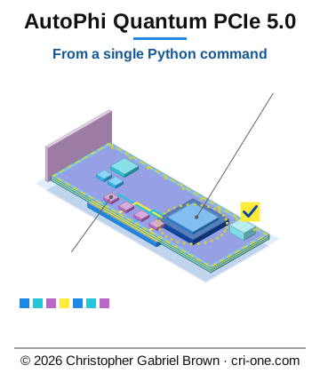
35-autophi-quantum-pcie5 packages the AutoPhi processor as a PCIe Gen5 card. The card claims the same nine-tech AutoPhi feature set, including LED Power Recycling and Quantum Battery — both exposed to the prior art summarized in the canonical doc.
Most relevant prior art for this project

Defensible angle

The card-level novelty is the integration into a standard PCIe Gen5 form factor with the full nine-tech stack — that's what the independent claim should hang on. Individual sub-features (LED recycle, QD battery) are already in the public record.

AutoPhi Quantum PCIe 5.0 — Photorealistic Render Specification

AutoPhi Quantum PCIe 5.0 — Photorealistic Render Specification

The APV19 tier board family

Project: 35 — AutoPhi Quantum PCIe 5.0

Document ID: APV19-RENDER-SPEC-001 · Rev: 2 (2026-08-13)

Geometry source: output/tier_boards/*.kicad_pcb — board outlines read directly

from the Edge.Cuts layer of each KiCad board file, which is fabrication truth.

Silicon and boards carry no .scad model. Their geometry lives in the KiCad board

file, and the board outline on Edge.Cuts is what the fab actually cuts to. Every

dimension below was measured from those files by _tools/scan_autophi.py and

cross-checked against KiCad's own geometry engine (`kicad-cli 10.0.5 pcb export

stats`).

> Rev 2 corrects Rev 1. The measurements were right; the interpretation was not.

> Rev 1 quoted the drawn envelope and called it the standard PCIe envelope, which it

> is not. It also described six boards where there are ten, and did not report that

> KiCad cannot resolve these outlines at all. See §1.

1. The tier family, measured

Ten boards, three form factors. All dimensions in mm.

Read the card body and the drawn envelope as two different numbers. The bodies

are exactly the PCIe mechanical standard. Each board then adds two features that sit

outside that rectangle, so the extent of the drawing is larger than the card itself.

Quoting the envelope as though it were the card is what Rev 1 got wrong.

The two extra features are identical on all ten boards:

  • a top-edge tab — 84.00 mm wide, centred on the top edge, standing 3.18 mm

(0.125 in) proud of the card body

  • a left-hand notch — 4.42 mm out beyond the card origin, 6.35 mm (0.25 in) tall,

at the bracket end

Both are deliberate drawn geometry, not stray marks. **The record does not say what

either is for.** Treat them as present and unexplained; do not invent a function.

Scale sanity, correctly stated. The PCIe standards are 312.00 × 111.15 mm

full-length full-height and 167.65 × 68.90 mm half-length low-profile. The bodies

here match both exactly, to the hundredth of a millimetre — these are real,

manufacturable card sizes. It is the envelope that is non-standard, because it

includes the tab and the notch.

Two defects to know about before rendering.

First, all ten boards carry a zero-length Edge.Cuts line at the origin, and it stops

KiCad resolving the outline: kicad-cli pcb export stats reports **"Dimensions:

unknown"** for every one of them. The figures above come from reading the geometry

directly, which is why they exist at all.

Second, and worse: the PCIe edge fingers are not on the board edge. J1 sits at

y = 100.99 on a body 111.15 mm tall, and the BUS_PCIexpress_x16 contacts end around

y = 106 — roughly 5 mm short of the edge they are supposed to terminate at. This is

visible directly in the reference render: the contact bar floats inboard of the bottom

edge with a strip of solder mask below it. A card-edge connector that does not reach the

card edge cannot enter a slot.

Taken together these outlines are drawable but not manufacturable — conclusive evidence

that these are placeholder boards, consistent with §8 and with the 46-component

population. Render them as design studies, never as cards that could be installed.

The family reads as a family. The five low-profile boards are dimensionally

identical, as are the two half-length full-height boards and the three full-length

boards. They differ by population, not outline — and per §8, not even by that. That is

the correct way to render them: same card, repeated. A render that makes MIC, MID and

MIN look like different products is wrong.

2. What is actually on the AQC board

Read the placement before describing the board. The footprint library for this

project contains a BGA-1536 at 95 × 90 mm, and it is tempting to assume the flagship

card carries it. It does not. Extracting placement from

APV19-BOARD-AQC.kicad_pcb gives 46 placed components and the largest is a QFN-48 at

7 × 7 mm. This is a sparse, connector-dominated carrier board, not a big-silicon

accelerator.

Population by family

That population — redrivers, ESD arrays, low-noise LDOs, an SFP112 cage and a PCIe

x16 edge — describes a signal-integrity carrier: it conditions and routes high-speed

lanes between an optical cage and the host slot. Render it as that.

3. Render 1 — the AQC carrier board

Photorealistic documentary photograph of a full-length PCIe carrier board, 312 mm long

and 111 mm tall, lying flat on a plain light grey bench and photographed from directly

overhead so the whole board is square in frame. Matte green solder mask with crisp

white silkscreen legends and reference designators. The board is notably sparse

long open stretches of mask with visible copper pour texture beneath, not a densely

populated card.

Along the lower long edge, the gold PCIe x16 edge connector with its keyed notch and

evenly plated contact fingers. At the left end, a metal SFP112 optical cage in bright

nickel, its port opening facing outward. Beside it, two black TE ribbon connectors

stacked one above the other, and a small white Molex header. A row of six M3 mounting

holes runs along the bottom edge at even 7 mm spacing, each with a plated ring.

Toward the right of centre, a single QFN-48 at 7 × 7 mm — the largest active part on

the board, a small matte black square with a visible thermal pad shadow. Scattered

between the connectors and the edge fingers, four small redriver ICs in fine-pitch

packages, eight tiny ESD protection arrays in SOT-sized packages clustered near the

high-speed paths, and a handful of regulators with their small ceramic and polymer

capacitors. Fine copper pours read as faint raised topography beneath the mask.

Palette of matte green mask, gold contacts, bright nickel cage, matte black packages,

white silkscreen.

4. Render 2 — the family, to scale

The family is three distinct cards, not ten products. Render one of each outline —

a full-length full-height card, a half-length full-height card, and a half-length

low-profile card — laid out together on a plain light grey bench, photographed from

directly overhead, aligned on one edge and evenly spaced so the size relationship reads

at a glance. No annotation, no scale bar — the objects carry the comparison.

Ten board files exist, but they resolve to only these three outlines (three full-length,

two half-length full-height, five low-profile) carrying an identical 46-component

population. Laying out ten near-identical cards would imply ten products and would be

wrong. If a group shot of the whole family is wanted, repeat the three outlines in their

3 / 2 / 5 counts and let the repetition be visible as repetition.

5. Camera and lighting

  • Phase One XF, 120 mm macro, f/11, focus stacked front to back
  • Tripod, precisely level, camera perpendicular to the bench, no perspective distortion
  • Plain technical documentation quality — the photograph taken for a manual or a filing

> The scene is ultra low energy: calm, still, quiet, nothing operating, no motion, no

> drama, no tension. Lighting is bright but deliberately boring: flat overcast noon or

> diffused fluorescent panel light bouncing off a white ceiling, soft shallow shadows,

> uniform exposure across the frame, no rim lights, no hard kickers, no cinematic

> contrast, no golden hour, no coloured gels, no dramatic falloff.

6. Negative prompt

> people, humans, hands, faces, glowing circuits, neon, blue LED glow, RGB lighting,

> holographic overlay, floating HUD, science fiction, motion, cooling fan spinning,

> cartoon, illustration, cgi plastic sheen, mirror-polished metal, text, watermark,

> logo, signature, oversaturated, dramatic lighting, rim light, cinematic contrast,

> lens flare, blown highlights, clipped shadows, tilted horizon, fisheye, motion blur,

> duplicated parts, warped geometry, floating components, gaming graphics card, RGB heatsink

> shroud, large heatsink, densely populated board, large central processor

Two failure modes specific to this product. Generators draw PCIe cards as *gaming

graphics cards* — shrouded, finned, backlit with a large heatsink. This is a bare,

sparsely populated carrier board with no shroud and no heatsink. And they over-populate:

46 components on a 312 mm board means large areas of empty mask, which is unusual-looking

and correct.

7. Generation settings

8. What the record does not contain

  • Placement extracted for all ten boards. Result: **every board carries the same 46

components**, all on the front side, at identical coordinates where the outline allows.

The five low-profile boards are indistinguishable in both outline and population. PEK,

PRO, AQC, UNI and VOL carry the same parts spread across a larger board. The tier

family therefore differs only by board outline — not by silicon, not by population.

  • This changes how the family should be rendered. It is one board design in three

sizes, not ten products. Any render implying different capability between MIC, MID and

MIN is wrong; any render giving AQC bigger silicon than MIN is wrong.

  • RESOLVED — the BGA-1536 is not on these boards because it lives in project 44.

It is U16 at (223.53, 93.15) on

44-autophi-pcie5-1536/blueprints/boards/01-qsfp28-optical/autophi-pcie5-qsfp28-optical-1536-FILLED-RICHER.kicad_pcb,

footprint AutoPhi:BGA-1536_95x90mm_P2.0mm. That board carries 525 components

against these boards' 46, and KiCad measures it cleanly at 256.625 × 111.95 mm.

**Project 44 is the real board of this line; the project 35 tier boards are

placeholders.** Render 44 as the flagship, not AQC. See 44/RENDER_SPECIFICATION.md.

  • Board stackup, now extracted: 6 copper layers (F.Cu, In1In4, B.Cu),

1.600 mm total thickness. Standard 1.6 mm card — render the edge accordingly, thin

relative to the connectors standing on it.

  • No solder mask colour is recorded. Matte green is assumed as the default.
  • No heatsink or thermal solution. At the power implied by a package this size,

a bare board is unlikely to be the shipping configuration, but nothing describes one.

  • No bracket geometry beyond its presence.

*Geometry measured by _tools/scan_autophi.py from Edge.Cuts, cross-checked against

kicad-cli 10.0.5 pcb export stats. Package sizes from the project's specification

documents, cross-confirmed against the STEP model at

40-autophi-bga256/interposer/autophi-1536-interposer.step, re-measured 2026-08-13 at

95.000 × 90.000 × 1.590 mm. (Rev 1 cited this model as living in 75-1536-interposer;

project 75 contains no STEP file.)*

Session Victory -- April 13, 2026

Session Victory -- April 13, 2026

> Christopher Gabriel Brown | CRI-ONE.COM | AutoPhi Quantum PCIe 5.0

What We Accomplished

Documentation (19 Markdown Files)

  • ARCHITECTURE.md -- Full system architecture, 10-layer stackup, net classes, RAG overview
  • STATUS.md -- Live routing metrics, DRC history, congestion analysis
  • CONTRIBUTING.md -- Development guide for returning to the project
  • README.md -- Complete project overview with 34-variant table and doc index
  • autophi_engine/README.md -- Engine API reference, build() pipeline, module inventory
  • blueprints/README.md -- Pipeline script guide, 5-stage flow, command cheatsheet
  • blueprints/VARIANTS.md -- Full 34-board catalog with connector categories
  • blueprints/ROUTING_PROCESS.md -- A* router pipeline, cost model, grid config
  • blueprints/ROUTING_TECHNIQUE_TARGET_FIRST.md -- Target-first routing technique
  • blueprints/ROUTING_TECHNIQUE_CONGESTION_HEATMAP.md -- Congestion detection and retry
  • blueprints/KICAD_PLUGIN.md -- 5 KiCad action plugins documented
  • blueprints/MANUFACTURING.md -- JLCPCB 10-layer fab spec
  • blueprints/rag-pcb-knowledge-base.md -- All 50+ RAG citations indexed
  • handoffs/HANDOFF_NOTES.md -- Manufacturing handoff with correct components
  • blueprints/TI_TIDA00423_COMPLETE_NETLIST.md -- 379 nets from original TI reference
  • Updated: ROUTING_DRC_MECHANISM.md, ROUTING_TECHNIQUE_ROW_LAYER_FANOUT.md, ROUTING_TECHNIQUE_DIFF_PAIR.md, SCHEMATIC_PROCESS.md

Routing Engine Fixes

  • Edge.Cuts boundary parser -- Fixed catastrophic bug where 189x70mm board was parsed as 1x0.5mm
  • Block-by-block parsing -- Replaced regex backtracking with depth-counted paren walker
  • Boundary enforcement -- 1.29M cells marked OUTSIDE, zero off-board traces
  • Best result: 376/430 nets (87.4%) on KiCad board, all within boundary
  • EasyEDA board: 311/417 nets (74.6%) -- first ever cross-format routing

EasyEDA Integration

  • easyeda_to_kicad.py -- Converts .eprj SQLite/NDJSON to valid .kicad_pcb
  • Parsed 212 components, 644 nets, 2,194 pad assignments from EasyEDA Pro format
  • Board outline with arcs properly converted
  • Successfully routed with our A* engine

Schematic Generation

  • generate_schematic.py rewritten with proper KiCad symbols
  • Capacitor plates, resistor bodies, IC boxes with real signal pin names
  • Power flags (GND, +3V3, +1V8, +1V0, +12V)
  • 35 schematics generated (1 main + 34 variants), 56MB total
  • 352 components, 323 nets, all cross-referenced

Magento Store -- 54 Products LIVE

  • 34 V19 schematic packages -- KiCad + BOM + netlist + README + product image
  • 10 V18 chip bundles -- 1,000 IC datasheets + foundry handoffs + specs
  • 10 V20 chip bundles -- 1,000 IC datasheets + GDSII + architecture docs
  • "Schematical Programs" category created (ID: 135)
  • All ZIPs uploaded via SSH/SFTP to cri-one.com server
  • All products created via Magento REST API
  • All product images uploaded
  • Cache flushed, indexes rebuilt
  • Live at: https://cri-one.com/store/schematical-programs.html

Netlist Exports

  • TI_TIDA00423_COMPLETE_NETLIST.md -- 379 nets categorized
  • TI_TIDA00423_COMPLETE_NETLIST.json -- Structured JSON
  • TI_TIDA00423_NETLIST_EASYEDA.net -- KiCad format for EasyEDA import
  • TI_TIDA00423_NETLIST_EASYEDA.csv -- 1,132 pin connections
  • TI_TIDA00423_NETLIST_EASYEDA.json -- EasyEDA JSON format

By the Numbers

What's Waiting for Round 2

  • PCB routing push to 95%+ (rip-and-reroute DDR blockers)
  • Per-variant PCB routing (propagate to all 34 boards)
  • Gerber export and manufacturing handoff
  • PCB layout packages for the Magento store
  • KiCad plugin DRC green annotation
  • EasyEDA round-trip (route in our engine, write back to .eprj)

The Sauce

The routing engine, RAG knowledge base, and EasyEDA converter stay local.

Only finished schematics and documentation ship to customers.

The proprietary algorithms are the competitive advantage -- they don't leave this machine.

"99.9% isn't finished... but 54 products on the store IS a win."

(c) 2026 Christopher Gabriel Brown. All rights reserved.

CRI-ONE.COM | AutoPhi Quantum PCIe 5.0 | Project 35

Routing Status

Routing Status

> Last updated: 2026-04-12

Current Best Result

Failed Nets by Category

Known Congestion Hotspots

All top-10 hotspots are at x = 243.7 mm in a 1.1 mm vertical strip:

Root cause: DDR address bus routes consume all channels at x=243.7mm, starving

PCIe cascaded copies and other nets that need to cross this region.

DRC Iteration History

Router Version History

Retry Pass Performance

The retry pass uses randomized pad ordering and layer cycling:

  • 87 nets entered retry after first pass
  • 18/87 attempted before budget expired (450s)
  • 17/18 recovered (94.4% success rate on attempted nets)
  • 69 nets never attempted -- ran out of time

Fix in progress: Triple retry budget (450s -> 1500s) so all 87 nets get a shot.

At 94% recovery rate, this should yield ~82 more nets -> ~429 routed (well past 404 target).

Next Steps

1. Extended retry budget (1500s) -- recover remaining failed nets

2. Rip-and-reroute DDR address blockers at x=243.7mm

3. Adaptive grid: 0.08mm in congested zones, 0.15mm elsewhere

4. Cascade routing: per-region grid/clearance/layer rules

5. Target: 95%+ routed, <50 DRC violations

6. Propagate routes to all 34 board variants

7. Package for Magento catalog on cri-one.com

autophiengine -- PCB Board Engine API

autophi_engine -- PCB Board Engine API

Core Python library for building AutoPhi PCIe 5.0 accelerator boards from parameters.

Quick Usage

from autophi_engine.engine import build

board = build(
    form_factor="HHHL",      # FHFL | FHHL | HHHL
    layers=12,                # 6, 8, or 12
    io_config="qb-energy",   # bracket connector config
)
board.save("output.kicad_pcb")
board.export_gerbers("gerbers/")
board.export_svg("preview.svg")
board.export_bom("bom.csv")

build() Function

def build(
    form_factor="HHHL",           # PCIe card form factor
    layers=12,                     # layer count (6, 8, 12)
    thickness=1.6,                 # board thickness in mm
    io_config="qb-energy",        # I/O bracket config from io_configs.py
    include_companion_chips=True,  # add thermal/LED/clock ICs
    silkscreen=None,               # dict: title, inventor, company, patents
    output_path=None,              # .kicad_pcb output path
) -> AutoPhiBoard

7-Step Internal Pipeline

1. Stackup -- Load layer configuration from rag/stackup.py

2. Board outline -- Generate PCIe card outline with mounting holes

3. Place components -- Zone-based placement from rag/components.py

4. Route traces -- Nearest-neighbour routing (MST-based)

5. GND stitching -- Place via reservoir across GND planes

6. Copper zones -- Generate copper pour polygons

7. Write PCB -- Emit KiCad v7 s-expression file

AutoPhiBoard Class

Returned by build(). Methods:

Package Structure

autophi_engine/
  engine.py          -- build() orchestrator, AutoPhiBoard class
  rag/               -- RAG knowledge base (cited constants)
    routing.py       -- 50+ citations, 18 net classes, A* config, JLCPCB specs
    components.py    -- 46 parts: BGA pin maps, body sizes, placement zones
    netlist.py       -- ALL_NETS dict, get_nets_for_component(), get_components_on_net()
    stackup.py       -- STACKUP_6L, STACKUP_8L, STACKUP_12L definitions
    io_configs.py    -- IO_CONFIGS for 34 bracket connectors
    placement.py     -- Placement zone rules and constraints
    rules.py         -- PCIE5, VIA, TRACE_WIDTH, MATERIAL, FORM_FACTORS
    superbase.py     -- Consolidated knowledge base
    ti_knowledge.py  -- TI TIDA-00423 reference data
    ti_adj_catalog.py -- TI application notes catalog
  layout/            -- Board geometry algorithms
    board.py         -- BoardOutline: form-factor outlines, mounting holes
    placer.py        -- Placer: zone-based component placement
    router.py        -- Router: nearest-neighbour trace routing, Track dataclass
    via_stitcher.py  -- ViaStitcher: GND via reservoir
    zone_filler.py   -- ZoneFiller: copper pour generation
  output/            -- File format exporters
    kicad_pcb.py     -- KiCadPCBWriter: v7 s-expression emitter
    gerber.py        -- export_gerbers(), export_drill(), export_svg(), validate()
  verify/            -- Design rule checking
    drc.py           -- DRC class: clearance checks, violation reporting

RAG Module Inventory

The rag/ directory contains the knowledge base that grounds every design decision.

Every constant is cited with source references (see ARCHITECTURE.md).

Helper Functions (routing.py)

classify_net(net_name) -> str          # "pcie_diff", "ddr_data", "default", etc.
class_params(class_name) -> dict       # width, clearance, via cost, priority
route_priority_key(net_name) -> int    # sort key (lower = route first)
layer_preference(class_name) -> str    # "F.Cu" or "B.Cu"
cite(tag) -> str                       # "[2][3] PCIe Gen3+ = 85 ohm diff..."
jlcpcb_min_trace_space(layers, cu_oz)  # (min_trace_mm, min_space_mm)
jlcpcb_impedance_feasible(z, diff)     # bool: can JLCPCB achieve this Z?

Form Factors

Related Documents

  • ../ARCHITECTURE.md -- System architecture overview
  • ../blueprints/README.md -- Pipeline scripts that consume this library
  • ../blueprints/rag-pcb-knowledge-base.md -- Full citation index

BGA + IO Placement Standard

BGA + IO Placement Standard

This project now uses a reusable anchor standard for the primary BGA and

left-edge IN/OUT connectors.

Canonical Coordinates

  • PCB edge left-bottom corner: (61.100, 114.650) mm
  • BGA center (U1): (141.500, 95.400) mm
  • BGA interchange window: 95.0 mm

Derived vector:

  • U1 - edge = (80.400, -19.250) mm

Connector Locking Rule

  • J2 and J3 keep fixed deltas from U1.
  • When U1 moves, both connectors move by the same translation vector.
  • This preserves IN/OUT spacing and makes the cluster reusable across boards.

Current offsets stored in placement.json:

  • J2 - U1 = (-75.817, -12.461) mm
  • J3 - U1 = (-75.817, 15.539) mm

Apply to Any Variant

Run from repository root:

python blueprints/apply_bga_io_standard.py `
  --edge-x 61.1 --edge-y 114.65 `
  --u1-x 141.5 --u1-y 95.4 `
  --bga-travel-mm 95

This updates:

  • blueprints/placement.json pinned centers (U1, J2, J3)
  • blueprints/placement.json metadata (_placement_standard)

The auto-placer (blueprints/auto_place.py) will then use those pinned

coordinates for all board variants.

AutoPhi 34-Board Fork — Pipeline Handoff

AutoPhi 34-Board Fork — Pipeline Handoff

Rebuild-everything doc for the TIDA-00423 → 34 AutoPhi I/O variants pipeline.

Written after the session on 2026-04-08. Everything described here runs from

D:\special\35-autophi-quantum-pcie5\blueprints\.

Goal

Fork the Texas Instruments TIDA-00423 PCIe Gen3 reference PCB into **34

product variants**, one per I/O bracket connector type, to pair with the

AutoPhi V19 Pinnacle chip catalog (1,060 SKUs) on cri-one.com. Every variant

must:

1. Preserve the TI card outline verbatim (PCI-SIG compliance).

2. Carry all 46 RAG-canonical parts from autophi_engine/rag/components.py.

3. Pack at ≥ 2 mm (back) / 4 mm (front) edge-to-edge clearance with zero

courtyard collisions.

4. Have its .kicad_pcb, SVG preview, and Magento catalog row emitted by a

one-command pipeline.

One-shot build

cd D:/special/35-autophi-quantum-pcie5
python blueprints/build_all.py

That runs: fork → SVG render → collision check → Magento CSV → preview HTML.

Output summary ends with OK: 34 boards, 0 collisions.

Pipeline stages

Key architectural decisions

1. Outline: flatten the retention tab

flatten_top_edge() strips every Edge.Cut segment with both endpoints above

y = -51.44 (the TI retention tab) and the stair-step connectors that

straddle the body boundary, then adds three new segments:

  • left vertical (-14.92, -58.45) → (-14.92, -51.44)
  • horizontal top (-14.92, -58.45) → (152.72, -58.45)
  • right vertical (152.72, -58.45) → (152.72, -51.44)

Result: the top of every board is a clean horizontal line.

2. Main body bounding box

After flatten, usable main body is X ∈ [-14.92, 152.72], Y ∈ [-51.44, -3.4].

Anything outside is either the PCIe-finger cutout (bottom) or outside the

board entirely.

3. Fixed parts (pre-packer)

  • U1 AutoPhi BGA-256 at (68.9, -29.5) 20×20 mm
  • U2-U5 DS160PR810 retimers at (46.9/90.9, -36.5/-22.5) 8×8 mm each
  • U6-U7 LP3878 LDOs at (113.9, -39.5/-29.5)
  • U20 iCE40UP5K at (113.9, -16.5) (renamed from U10)
  • J1 PCIe x16 fingers at (72, 6.87)
  • J2/J3 I/O connectors at (-6.92, -42) and (-6.92, -14), rotated 90°,

flush with the left short edge (Edge.Cut at x = -14.92). Anchor x is

-14.92 + 8 mm (shield half-width) so pads hit the edge exactly.

  • MH1-MH4 around U1 at (±15, ±15) offset
  • MH5 at (5, -48), MH6 at (148, -48)
  • 128 decoupling caps in rings around U2-U5 (32 each), 20 around U1
  • 8 bulk caps around U6/U7

4. RT / TP / D placements (post-fix)

  • RT1-RT8 NTC thermistors at inter-chip gaps:

(55/83/103, -33), (55/83/103, -26), (36, -33), (36, -26)

  • TP1-TP6 at (5,10,15,20,25,30; -28) in the left corridor between J2/J3
  • D1-D4 power LEDs at (143, -40/-35/-30/-25)

5. Option-A packer (37 extra RAG canonical parts)

Zone-packer in fork_ti_board.py:build_components:

CLEARANCE_F = 4.0   # front side (F.Cu)
CLEARANCE_B = 2.0   # back side  (B.Cu)

Packer computes real pad bboxes — declared w/h in the part table is

advisory. _real_pad_bbox(pads) measures actual pad extents so _soic_pads

and _qfn_pads don't overflow zones.

Front mid row @ y=-11, ranges [(4,41), (52,85), (96,109), (120,138)]:

  • Big parts: U8, U40, U41, U43, U44, J4, TEC1, TEC2, LED1

Back top row @ y=-47, ranges [(4,41), (52,85), (96,109), (120,146)]:

  • Power/telemetry: U12-U14, U21-U24, U25-U30, U42, U29, U30, J10, J11

Back mid row @ y=-6, ranges [(4,148)]:

  • SW1-SW8 + U45-U52 ESD arrays

Back terminator rows @ y=-30 and y=-28.5, ranges [(4,148)], clearance 1.5:

  • RT9-RT34 (26× 49.9Ω 0402 under U1 BGA — back is empty there)

Zone left edges start at x=4 (not x=2) so the packer never touches J3's

shield pad at x=1.08.

6. Side-split rule

Front side gets big / visible / connector-bearing parts. Back side gets

small SMD / config / terminator parts. This lets the front keep 4 mm

clearance (the physical density limit of the HHHL main body).

7. Renderer colors

render_board_svg.py parses the footprint's (layer "...") and draws:

  • Front parts: gold pads (#e7b74d) + white courtyard outlines
  • Back parts: cyan pads (#5dc1d9) + muted cyan outlines
  • Every SMD gets a bbox outline so collisions are visible at a glance.

8. Collision detector

Inline in build_all.py. Uses parse_footprints() + rotated pad bboxes,

ignores C* refs (cap rings are dense by design), and only flags same-side

overlaps. Output: 0 collisions on all 34 boards.

Known gotchas (bugs we hit and fixed, don't repeat)

Open TODOs

1. Real footprints from Ultra Librarian. Most Option-A parts use

placeholder tiny_pads() bodies. Swap for real ones from

<https://www.ultralibrarian.com/cad-vendors/kicad/>.

2. kicad-cli compatibility. Fix the fork's sexpr so native KiCad 10 can

open the .kicad_pcb files (needed for gerber export).

3. Route traces. build_nets() defines 232 nets but no traces are

actually routed. Add autophi_engine/layout/router.py-style routing.

4. Narrow related_skus per tier. Currently every board lists all 1060

chip SKUs. Should probably be per-tier (SEE→all Seed chips, etc.).

5. Variant Y-coordinate for goal image match. The SMD-15-2026 product

image has a specific aesthetic the user wants matched — still waiting on

a screenshot to diff against.

6. Prices calibration. Current $15k-50k tiers were derived from

io_configs.py anchors + category floors. User may want to override.

File map

blueprints/
├── fork_ti_board.py         # main forker (flatten + place + write)
├── generate_pcb.py           # 34 IO_CONNECTOR_DEFS + IO_BOARD_NAMES
├── render_board_svg.py       # custom Python SVG renderer (bypasses kicad-cli)
├── placement.json            # fixed-part coordinates (U1, J1, J2, J3, etc.)
├── build_magento_34_boards.py  # RAG-grounded Magento CSV builder
├── build_all.py              # one-shot pipeline runner (fork→svg→check→csv)
├── HANDOFF.md                # this file
└── boards/
    ├── preview-34.html       # grid viewer of all 34 SVGs
    ├── manifest_34.csv       # board-level SKU+name+path table
    ├── magento_import_34.csv # full Magento product rows
    └── NN-<key>/
        ├── autophi-pcie5-<key>.kicad_pcb
        └── preview.svg

Memory

The user's durable-memory note at

C:\Users\Administrator\.claude\projects\D--special-35-autophi-quantum-pcie5\memory\feedback_consult_rag_each_step.md

says: review the RAG at every step, not just generation. Before making

changes to any of the stages above, read the relevant

autophi_engine/rag/*.py file first.

KiCad Plugin -- AutoPhi Router

KiCad Plugin -- AutoPhi Router

5 action plugins for KiCad 10.0 that bring AutoPhi routing tools into the editor.

Location: C:\Users\Administrator\Documents\KiCad\10.0\scripting\plugins\autophi_router\__init__.py

Plugin Actions

1. AutoPhi: Route Board

Opens a dialog with routing settings:

Currently delegates to external python blueprints/auto_route.py for the full

routing run. The dialog logs settings and provides a launch point.

2. AutoPhi: Via Cascade

Places via-in-pad on BGA and DDR pads with distance-based 4-layer cascade:

Core refs: U1, U2-U5, U8, U63-U66, J1.

3. AutoPhi: DRC Check

Basic post-route clearance verification:

  • Via-to-via center distance check
  • Min clearance: 0.09 mm (JLCPCB 6L)
  • Caps at 1,000 violations for performance
  • Reports total violation count

4. AutoPhi: Smart Place

Moves small bypass caps near their connected IC power pins:

  • Targets: C_0201, C_0402, C_0805, R_0402, R_0805
  • Finds the IC pad connected to each passive via shared net
  • Places passive 2.0mm from the IC pad
  • All placed components stay within the board boundary

5. AutoPhi: Unroute All

Strips all tracks and vias from the board. Reports counts removed.

Use before a full re-route.

Installation

1. Copy __init__.py to KiCad scripting plugins directory:

   C:\Users\<user>\Documents\KiCad\10.0\scripting\plugins\autophi_router\__init__.py

2. Restart KiCad

3. Plugins appear under Tools > External Plugins > AutoPhi Router

4. Or use the toolbar buttons (if show_toolbar_button = True)

KiCad 10 API Notes

  • Via type constant changed: code uses try/except for VIATYPE_THROUGH -> VIA_THROUGH fallback
  • pcbnew.FromMM() / pcbnew.ToMM() for coordinate conversion
  • pcbnew.VECTOR2I() for position setting
  • pcbnew.Refresh() after board modifications

Relationship to CLI Scripts

The plugin provides quick access to individual tools. For production routing

of all 34 board variants, use the CLI pipeline:

python blueprints/auto_route.py "board.kicad_pcb" --grid 0.12 --timeout 15

Manufacturing Specification

Manufacturing Specification

> Target fab: JLCPCB | 10-layer | 1.6mm | ENIG finish

Target Fab Houses

10-Layer Stackup

Material: Megtron 6 (Dk=3.15, Df=0.002) with HVLP2 copper foil.

Total thickness: 1.6 mm (standard JLCPCB).

Design Rules

Impedance Targets

JLCPCB controlled impedance is free on multilayer boards (tick-box enable).

Via Policy

Layer-specific vias: Standard through-drill at JLCPCB, but KiCad's (layers "X" "Y")

directive means the via only connects the specified layers. No HDI process needed.

Surface Finish

ENIG (Electroless Nickel Immersion Gold) -- required for BGA pads at 1.0mm pitch.

Board Boundary

All traces, vias, and components must stay within the Edge.Cuts board outline.

The router rasterizes the outline and marks all cells outside as OUTSIDE (blocked).

Mounting holes (MH1-MH6) have 3mm keepout zones on all layers.

Assembly Notes

Known Constraints

  • No blind/buried vias (JLCPCB standard process) -- use layer-specific through-vias instead
  • Max hole aspect ratio 10:1 (1.6mm board -> 0.16mm min drill, we use 0.20mm)
  • BGA requires ENIG finish (HASL/OSP not flat enough for 1.0mm pitch)
  • All components and traces must remain within board outline boundaries
  • No traces under mounting holes (3mm keepout radius on all layers)

Blueprints -- Pipeline Scripts

Blueprints -- Pipeline Scripts

33 Python scripts (~14,000 lines) that transform the TI TIDA-00423 reference design

into 34 routed AutoPhi PCIe 5.0 product variants.

One-Command Build

python blueprints/build_all.py

This runs all 5 stages: fork -> place -> route -> DRC -> export.

Pipeline Stages

Stage 0: Schematic     Stage 1: Fork          Stage 2: Place
generate_schematic.py  fork_ti_board.py       place_passives_clustered.py
skidl_autophi_v3.py    ti_net_mapping.py      resolve_collisions.py
                       generate_pcb.py        snap_passives.py
        |                     |                      |
        v                     v                      v
  .kicad_sch            34x .kicad_pcb         Caps wrapped around ICs
  + netlist             (one per variant)       Collisions resolved
                              |
                              v
                       Stage 3: Route          Stage 4: Verify
                       auto_route.py           drc_check.py
                       propagate_routes.py
                              |                      |
                              v                      v
                       Routed .kicad_pcb       Violation report
                       + route cache
                              |
                              v
                       Stage 5: Export
                       render_board_svg.py     -> SVG previews
                       build_magento_34_boards.py -> Magento CSV
                       domino_pipeline.py      -> Product packaging

Command Cheatsheet

# Route a board (preserves existing wires)
python blueprints/auto_route.py "boards/01-qsfp28-optical/autophi-pcie5-qsfp28-optical.kicad_pcb" \
  --exclude-refs J2,J3,J4 --grid 0.12 --timeout 15

# Unwire and reroute from scratch
python blueprints/auto_route.py "boards/01-.../....kicad_pcb" --unwire

# DRC check
python blueprints/drc_check.py "boards/01-.../....kicad_pcb"

# Render SVG preview
python blueprints/render_board_svg.py "boards/01-.../....kicad_pcb"

# Place passives around ICs
python blueprints/place_passives_clustered.py "boards/01-.../....kicad_pcb"

# Resolve component collisions
python blueprints/resolve_collisions.py "boards/01-.../....kicad_pcb"

# Export to Specctra DSN (for Freerouting interop)
python blueprints/kicad_to_dsn.py "boards/01-.../....kicad_pcb" --exclude-refs J2,J3,J4

# Build all 34 variants
python blueprints/build_all.py

# One-click schematic + all I/O variant sync
python blueprints/one_click_schematic_io_sync.py --source 01-qsfp28-optical

# One-click sync with U1 large-BGA override from 40-autophi-bga
python blueprints/one_click_schematic_io_sync.py --source 01-qsfp28-optical \
  --u1-pinmap "d:\special\40-autophi-bga\pinmaps\AUTOPHI_BGA1536_pinmap_working.csv" \
  --u1-value "AUTOPHI_BGA1536" \
  --u1-footprint "AutoPhi:BGA-1536_95x90mm_P2.0mm"

# Propagate core routes to all variants
python blueprints/propagate_routes.py

# Generate Magento import CSV
python blueprints/build_magento_34_boards.py

Script Reference

Core Pipeline

Placement

Routing Support

Netlist and Schematic

Output and Export

Utilities

Board Variant Directory

See VARIANTS.md for the full 34-board catalog.

blueprints/boards/
  01-qsfp28-optical/    -- Primary development board
  02-sfp-optical/
  ...
  34-audio-trs/
  magento_import_34.csv -- Magento product import
  manifest_34.csv       -- Variant manifest
  preview-34.html       -- 34-board grid viewer
  interactive_editor.html -- Web-based layout editor

Routing Technique Documentation

  • ROUTING_PROCESS.md -- Pipeline overview
  • ROUTING_DRC_MECHANISM.md -- DRC-safe mechanism (8 failure iterations)
  • ROUTING_TECHNIQUE_DIFF_PAIR.md -- P+N differential pair routing
  • ROUTING_TECHNIQUE_ROW_LAYER_FANOUT.md -- BGA row-to-layer
  • ROUTING_TECHNIQUE_CACHED_INCREMENTAL.md -- Cache + incremental
  • ROUTING_TECHNIQUE_TARGET_FIRST.md -- Target-first routing
  • ROUTING_TECHNIQUE_CONGESTION_HEATMAP.md -- Congestion analysis

Other Documentation

  • MANUFACTURING.md -- JLCPCB fab specifications
  • KICAD_PLUGIN.md -- KiCad action plugin guide
  • SCHEMATIC_PROCESS.md -- Schematic generation pipeline
  • rag-pcb-knowledge-base.md -- Full RAG citation index
  • HANDOFF.md -- Pipeline handoff guide

This archive contains 82 documents; 69 more beyond this preview. The complete folder ships as the product.

Write Your Own Review
You're reviewing:35-autophi-quantum-pcie5
Copyright © 2009 Christopher Gabriel Brown