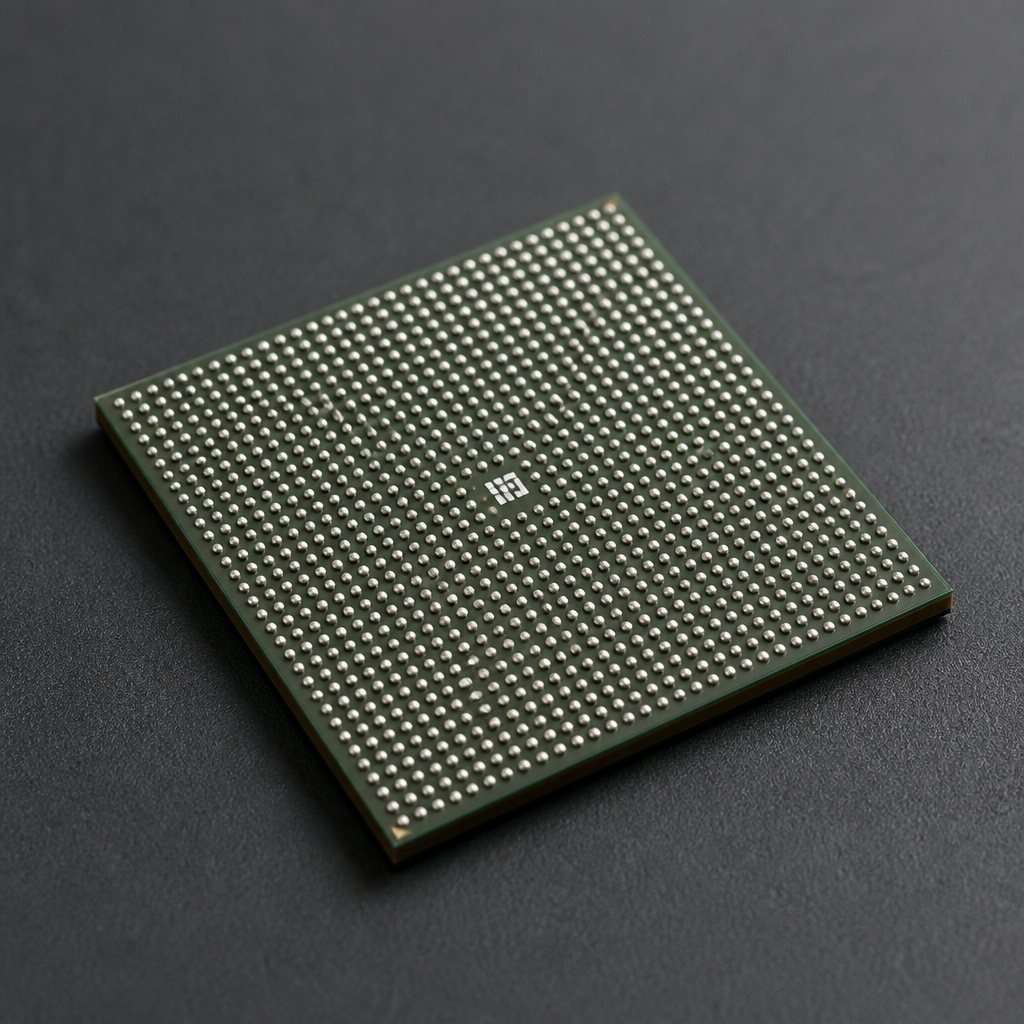
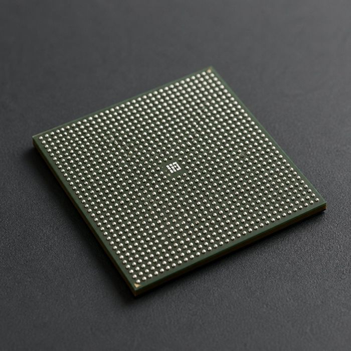
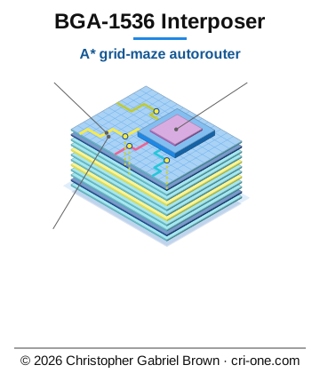
75-1536-interposer

$99,999,999.00
In stock
SKU
2106
Asset valuation: $40,000,000,000. This project now uses a reusable anchor standard for the primary BGA and left-edge IN/OUT connectors. - PCB edge left-bottom corner: (61.100, 114.650) mm - BGA center (U1): (141.500, 95.400) mm - BGA interchange window: 95.0 mm

Valuation

Generous asset valuation: $40,000,000,000. The listed price is the platform maximum; acquisition at valuation is handled by direct enquiry.

BGA + IO Placement Standard

BGA + IO Placement Standard

This project now uses a reusable anchor standard for the primary BGA and

left-edge IN/OUT connectors.

Canonical Coordinates

  • PCB edge left-bottom corner: (61.100, 114.650) mm
  • BGA center (U1): (141.500, 95.400) mm
  • BGA interchange window: 95.0 mm

Derived vector:

  • U1 - edge = (80.400, -19.250) mm

Connector Locking Rule

  • J2 and J3 keep fixed deltas from U1.
  • When U1 moves, both connectors move by the same translation vector.
  • This preserves IN/OUT spacing and makes the cluster reusable across boards.

Current offsets stored in placement.json:

  • J2 - U1 = (-75.817, -12.461) mm
  • J3 - U1 = (-75.817, 15.539) mm

Apply to Any Variant

Run from repository root:

python blueprints/apply_bga_io_standard.py `
  --edge-x 61.1 --edge-y 114.65 `
  --u1-x 141.5 --u1-y 95.4 `
  --bga-travel-mm 95

This updates:

  • blueprints/placement.json pinned centers (U1, J2, J3)
  • blueprints/placement.json metadata (_placement_standard)

The auto-placer (blueprints/auto_place.py) will then use those pinned

coordinates for all board variants.

AutoPhi 34-Board Fork — Pipeline Handoff

AutoPhi 34-Board Fork — Pipeline Handoff

Rebuild-everything doc for the TIDA-00423 → 34 AutoPhi I/O variants pipeline.

Written after the session on 2026-04-08. Everything described here runs from

D:\special\35-autophi-quantum-pcie5\blueprints\.

Goal

Fork the Texas Instruments TIDA-00423 PCIe Gen3 reference PCB into **34

product variants**, one per I/O bracket connector type, to pair with the

AutoPhi V19 Pinnacle chip catalog (1,060 SKUs) on cri-one.com. Every variant

must:

1. Preserve the TI card outline verbatim (PCI-SIG compliance).

2. Carry all 46 RAG-canonical parts from autophi_engine/rag/components.py.

3. Pack at ≥ 2 mm (back) / 4 mm (front) edge-to-edge clearance with zero

courtyard collisions.

4. Have its .kicad_pcb, SVG preview, and Magento catalog row emitted by a

one-command pipeline.

One-shot build

cd D:/special/35-autophi-quantum-pcie5
python blueprints/build_all.py

That runs: fork → SVG render → collision check → Magento CSV → preview HTML.

Output summary ends with OK: 34 boards, 0 collisions.

Pipeline stages

Key architectural decisions

1. Outline: flatten the retention tab

flatten_top_edge() strips every Edge.Cut segment with both endpoints above

y = -51.44 (the TI retention tab) and the stair-step connectors that

straddle the body boundary, then adds three new segments:

  • left vertical (-14.92, -58.45) → (-14.92, -51.44)
  • horizontal top (-14.92, -58.45) → (152.72, -58.45)
  • right vertical (152.72, -58.45) → (152.72, -51.44)

Result: the top of every board is a clean horizontal line.

2. Main body bounding box

After flatten, usable main body is X ∈ [-14.92, 152.72], Y ∈ [-51.44, -3.4].

Anything outside is either the PCIe-finger cutout (bottom) or outside the

board entirely.

3. Fixed parts (pre-packer)

  • U1 AutoPhi BGA-256 at (68.9, -29.5) 20×20 mm
  • U2-U5 DS160PR810 retimers at (46.9/90.9, -36.5/-22.5) 8×8 mm each
  • U6-U7 LP3878 LDOs at (113.9, -39.5/-29.5)
  • U20 iCE40UP5K at (113.9, -16.5) (renamed from U10)
  • J1 PCIe x16 fingers at (72, 6.87)
  • J2/J3 I/O connectors at (-6.92, -42) and (-6.92, -14), rotated 90°,

flush with the left short edge (Edge.Cut at x = -14.92). Anchor x is

-14.92 + 8 mm (shield half-width) so pads hit the edge exactly.

  • MH1-MH4 around U1 at (±15, ±15) offset
  • MH5 at (5, -48), MH6 at (148, -48)
  • 128 decoupling caps in rings around U2-U5 (32 each), 20 around U1
  • 8 bulk caps around U6/U7

4. RT / TP / D placements (post-fix)

  • RT1-RT8 NTC thermistors at inter-chip gaps:

(55/83/103, -33), (55/83/103, -26), (36, -33), (36, -26)

  • TP1-TP6 at (5,10,15,20,25,30; -28) in the left corridor between J2/J3
  • D1-D4 power LEDs at (143, -40/-35/-30/-25)

5. Option-A packer (37 extra RAG canonical parts)

Zone-packer in fork_ti_board.py:build_components:

CLEARANCE_F = 4.0   # front side (F.Cu)
CLEARANCE_B = 2.0   # back side  (B.Cu)

Packer computes real pad bboxes — declared w/h in the part table is

advisory. _real_pad_bbox(pads) measures actual pad extents so _soic_pads

and _qfn_pads don't overflow zones.

Front mid row @ y=-11, ranges [(4,41), (52,85), (96,109), (120,138)]:

  • Big parts: U8, U40, U41, U43, U44, J4, TEC1, TEC2, LED1

Back top row @ y=-47, ranges [(4,41), (52,85), (96,109), (120,146)]:

  • Power/telemetry: U12-U14, U21-U24, U25-U30, U42, U29, U30, J10, J11

Back mid row @ y=-6, ranges [(4,148)]:

  • SW1-SW8 + U45-U52 ESD arrays

Back terminator rows @ y=-30 and y=-28.5, ranges [(4,148)], clearance 1.5:

  • RT9-RT34 (26× 49.9Ω 0402 under U1 BGA — back is empty there)

Zone left edges start at x=4 (not x=2) so the packer never touches J3's

shield pad at x=1.08.

6. Side-split rule

Front side gets big / visible / connector-bearing parts. Back side gets

small SMD / config / terminator parts. This lets the front keep 4 mm

clearance (the physical density limit of the HHHL main body).

7. Renderer colors

render_board_svg.py parses the footprint's (layer "...") and draws:

  • Front parts: gold pads (#e7b74d) + white courtyard outlines
  • Back parts: cyan pads (#5dc1d9) + muted cyan outlines
  • Every SMD gets a bbox outline so collisions are visible at a glance.

8. Collision detector

Inline in build_all.py. Uses parse_footprints() + rotated pad bboxes,

ignores C* refs (cap rings are dense by design), and only flags same-side

overlaps. Output: 0 collisions on all 34 boards.

Known gotchas (bugs we hit and fixed, don't repeat)

Open TODOs

1. Real footprints from Ultra Librarian. Most Option-A parts use

placeholder tiny_pads() bodies. Swap for real ones from

<https://www.ultralibrarian.com/cad-vendors/kicad/>.

2. kicad-cli compatibility. Fix the fork's sexpr so native KiCad 10 can

open the .kicad_pcb files (needed for gerber export).

3. Route traces. build_nets() defines 232 nets but no traces are

actually routed. Add autophi_engine/layout/router.py-style routing.

4. Narrow related_skus per tier. Currently every board lists all 1060

chip SKUs. Should probably be per-tier (SEE→all Seed chips, etc.).

5. Variant Y-coordinate for goal image match. The SMD-15-2026 product

image has a specific aesthetic the user wants matched — still waiting on

a screenshot to diff against.

6. Prices calibration. Current $15k-50k tiers were derived from

io_configs.py anchors + category floors. User may want to override.

Autorouter (auto_route.py)

Grid A* routing writes the .kicad_pcb in place. After each successful write,

the script runs kicad-cli pcb drc when the CLI is on PATH or under

typical Windows KiCad install paths (override with env KICAD_CLI). Use

--no-drc to skip (e.g. CI without KiCad). The second-pass retry of failed

nets follows R.A_STAR["backoff_if_fail"] in autophi_engine/rag/routing.py.

CI: GitHub Actions .github/workflows/ci.yml runs pytest tests/ on

push/PR (fast unit tests; integration is skipped by default). Weekly /

manual integration.yml sets AUTOPHI_INTEGRATION=1 for the optional

route_board smoke test.

Pad order: Target-first chaining (route connector/retimer before BGA) uses

R.NET_PAD_ORDER["target_first_refs"] (default U1). Override with

--target-first-refs REFS or disable with --no-target-first.

Global + detailed: R.GLOBAL_ROUTE runs a coarse tile BFS on the

start layer, builds an inflated fine-cell corridor, then runs detailed A\*

inside it; if that fails, it falls back to full-grid A\*. Disable with

--no-global-route.

Easy button (Windows): from repo root, run easy.cmd (double-click or in a terminal)

for a small menu (tests / integration / route a board). Same as .\scripts\easy.ps1

with arguments test, integration, or route. The first test run installs pytest

via pip if needed (requirements-dev.txt); or run easy.cmd deps first.

File map

blueprints/
├── fork_ti_board.py         # main forker (flatten + place + write)
├── generate_pcb.py           # 34 IO_CONNECTOR_DEFS + IO_BOARD_NAMES
├── render_board_svg.py       # custom Python SVG renderer (bypasses kicad-cli)
├── placement.json            # fixed-part coordinates (U1, J1, J2, J3, etc.)
├── build_magento_34_boards.py  # RAG-grounded Magento CSV builder
├── build_all.py              # one-shot pipeline runner (fork→svg→check→csv)
├── HANDOFF.md                # this file
└── boards/
    ├── preview-34.html       # grid viewer of all 34 SVGs
    ├── manifest_34.csv       # board-level SKU+name+path table
    ├── magento_import_34.csv # full Magento product rows
    └── NN-<key>/
        ├── autophi-pcie5-<key>.kicad_pcb
        └── preview.svg

Memory

The user's durable-memory note at

C:\Users\Administrator\.claude\projects\D--special-35-autophi-quantum-pcie5\memory\feedback_consult_rag_each_step.md

says: review the RAG at every step, not just generation. Before making

changes to any of the stages above, read the relevant

autophi_engine/rag/*.py file first.

Integration parts — “today” PCs vs “tomorrow” servers

Integration parts — “today” PCs vs “tomorrow” servers

Canonical narrative: D:\special\18-autophi-future · Engineering + RAG: D:\special\35-autophi-quantum-pcie5 · This tree: D:\special\39-autophi-pcie5.

This document names what must exist on the card and what the host must provide so the accelerator integrates into real machines—not only a schematic fantasy.

Sourcing policy: AutoPhi Quantum (U1) is the only custom / non–catalog silicon you own; every other line item is chosen from commercial vendors (TI where the reference design calls for it—e.g. DS80PCI810—plus DRAM, connectors, passives, PMICs, etc. from their normal supply chains and MPNs).

A. On-card silicon & companions (from 35 / ARCHITECTURE.md)

Machine-readable rows: integration_parts_today_tomorrow.json (same folder).

B. “Today” — typical workstation / white-box PC

Host must have

  • [ ] Open PCIe ×16 slot (electrical + mechanical: full-height vs low-profile matches bracket).
  • [ ] Enough continuous +12 V / +3.3 V / +3.3 V AUX headroom for your power map (see board power nets in schematic).
  • [ ] Air path: case fans or GPU-style shroud if TDP is not trivial.
  • [ ] OS + driver path: if you expose standard PCIe class devices, plan signed driver or inbox class; if custom, plan attestation story.

You ship / certify

  • [ ] One bracket + faceplate variant that matches retail PCs.
  • [ ] Thermal interface spec (max °C at case inlet, throttle policy if any).
  • [ ] Labeling + regulatory bucket (FCC/CE as applicable).

C. “Tomorrow” — rack servers / data-center hosts

Host must have

  • [ ] Same electrical lane budget (or deliberate bifurcation / retimer path if you split the link).
  • [ ] Cooling: front-to-rear airflow, inlet temperature class, N+1 fan policy if required.
  • [ ] BMC / inventory: FRU EEPROM or SMBus plan if operators must discover the card without opening the chassis.
  • [ ] Security: firmware update channel, secure boot interaction if you have option ROM or management endpoint.

You ship / certify

  • [ ] Server-grade bracket / EMI finger stock if the variant needs it.
  • [ ] Vibration and shock notes for heavy heatsinks or optical modules.
  • [ ] Multi-tenant story: noisy neighbour on the same PCIe root complex (QoS, SR-IOV only if you actually implement it).

D. Next concrete engineering steps (repo)

1. Bind U1 to a real part number or FPGA + carrier plan—until then, “integration” stops at retimer+DDR+edge.

2. Pull MPNs for passives / PMICs from board_inventory.json into the JSON (or a generated BOM CSV from KiCad).

3. Re-run Update PCB from Schematic after any GND / MH fixes so host-side DRC matches reality.

4. Align stackup in KiCad with ARCHITECTURE.md (10-layer vs 18-layer: pick one truth per product generation).

This file is meant to evolve. When U1 is frozen, add a row in the JSON with mpn, manufacturer, and lifecycle.

KiCad Plugin -- AutoPhi Router

KiCad Plugin -- AutoPhi Router

7 action plugins for KiCad 10.0 that bring AutoPhi routing tools into the editor.

Source (repo): blueprints/kicad_plugin/autophi_router/__init__.py

Install: copy that autophi_router folder to

Documents/KiCad/10.0/scripting/plugins/autophi_router/

Plugin Actions

1. AutoPhi: Route Board

Opens a dialog with routing settings:

Currently delegates to external python blueprints/auto_route.py for the full

routing run. The dialog logs settings and provides a launch point.

If Route Board “does nothing” or never finishes: KiCad’s sys.executable is

often kicad.exe, not Python. The plugin now starts python from your PATH

(Windows: also tries the py -3 launcher) so auto_route.py actually runs.

To force an interpreter, set the environment variable AUTOPHI_PYTHON to

the full path of python.exe (e.g. a venv: D:\…\project\.venv\Scripts\python.exe).

You must be able to run python blueprints\auto_route.py from a terminal in

the repository root with that same Python (imports autophi_engine).

A separate console may open on Windows so you can see router output; when it

exits, reload the .kicad_pcb in Pcbnew (file was overwritten on disk).

2. AutoPhi: Via Cascade

Implemented in the plugin (not stub): for each via, measures distance

from the via position to the nearest anchor footprint in this set:

U1, U2–U5, U8, U63–U66, J1. Then sets the via layer pair (F.Cu to inner,

or F.Cu to B.Cu) as follows.

If you pre-select vias, only the selection is updated; otherwise every via

on the board is updated. Microvias are skipped. The CLI router still

applies its own row-to-layer policy during auto_route.py; this action is

for interactive post-adjustment in Pcbnew. Ensure blind/buried vias are

allowed in Board Setup for inner layer spans, or the engine may not apply

all pairs; failed counts are shown in the dialog.

3. AutoPhi: DRC Check

Basic post-route clearance verification:

  • Via-to-via center distance check
  • Min clearance: 0.09 mm (JLCPCB 6L)
  • Caps at 1,000 violations for performance
  • Reports total violation count

4. AutoPhi: Smart Place

Moves small bypass caps near their connected IC power pins:

  • Targets: C_0201, C_0402, C_0805, R_0402, R_0805
  • Finds the IC pad connected to each passive via shared net
  • Places passive 2.0mm from the IC pad
  • All placed components stay within the board boundary

5. AutoPhi: Unroute All

Strips all tracks and vias from the board. Reports counts removed.

Use before a full re-route.

6. AutoPhi: Party Grid Place

Fast placement helper after a messy netlist / import (many footprints stacked at

the board origin, hard to see, “no airwires” confusion):

Sorts by reference (C2 before C10). Does not add footprints missing from the PCB;

fix the schematic / Update PCB from schematic first, then use this to unstack what

landed on the board.

7. AutoPhi: Fancy Silk Outline

Adds a halo (duplicate PCB_TEXT strokes) around board-level silk text on

F.SilkS / B.SilkS, rotated with the original lettering so the outline tracks

rotated labels. Optional: turn on KiCad silk knockout for footprint

Reference/Value when those fields sit on silk (improves contrast on soldermask).

Dialog controls: outline offset (mm), 8- or 16-way ring, extra halo stroke width,

and the knockout checkbox. Uses pcbnew.COMMIT when available so a single Undo

reverts the halo pass.

Installation

1. Copy the folder blueprints/kicad_plugin/autophi_router/ into the KiCad

scripting plugins directory (so __init__.py ends up at):

   C:\Users\<user>\Documents\KiCad\10.0\scripting\plugins\autophi_router\__init__.py

2. Restart KiCad

3. Plugins appear under Tools > External Plugins > AutoPhi Router

4. Or use the toolbar buttons (if show_toolbar_button = True)

KiCad 10 API Notes

  • Via type constant changed: code uses try/except for VIATYPE_THROUGH -> VIA_THROUGH fallback
  • pcbnew.FromMM() / pcbnew.ToMM() for coordinate conversion
  • pcbnew.VECTOR2I() for position setting
  • pcbnew.Refresh() after board modifications

Relationship to CLI Scripts

The plugin provides quick access to individual tools. For production routing

of all 34 board variants, use the CLI pipeline:

python blueprints/auto_route.py "board.kicad_pcb" --grid 0.12 --timeout 15

Manufacturing Specification

Manufacturing Specification

> Target fab: JLCPCB | 10-layer | 1.6mm | ENIG finish

Target Fab Houses

10-Layer Stackup

Material: Megtron 6 (Dk=3.15, Df=0.002) with HVLP2 copper foil.

Total thickness: 1.6 mm (standard JLCPCB).

Design Rules

Impedance Targets

JLCPCB controlled impedance is free on multilayer boards (tick-box enable).

Via Policy

Layer-specific vias: Standard through-drill at JLCPCB, but KiCad's (layers "X" "Y")

directive means the via only connects the specified layers. No HDI process needed.

Surface Finish

ENIG (Electroless Nickel Immersion Gold) -- required for BGA pads at 1.0mm pitch.

Board Boundary

All traces, vias, and components must stay within the Edge.Cuts board outline.

The router rasterizes the outline and marks all cells outside as OUTSIDE (blocked).

Mounting holes (MH1-MH6) have 3mm keepout zones on all layers.

Assembly Notes

Known Constraints

  • No blind/buried vias (JLCPCB standard process) -- use layer-specific through-vias instead
  • Max hole aspect ratio 10:1 (1.6mm board -> 0.16mm min drill, we use 0.20mm)
  • BGA requires ENIG finish (HASL/OSP not flat enough for 1.0mm pitch)
  • All components and traces must remain within board outline boundaries
  • No traces under mounting holes (3mm keepout radius on all layers)

Blueprints -- Pipeline Scripts

Blueprints -- Pipeline Scripts

33 Python scripts (~14,000 lines) that transform the TI TIDA-00423 reference design

into 34 routed AutoPhi PCIe 5.0 product variants.

One-Command Build

python blueprints/build_all.py

This runs all 5 stages: fork -> place -> route -> DRC -> export.

Pipeline Stages

Stage 0: Schematic     Stage 1: Fork          Stage 2: Place
generate_schematic.py  fork_ti_board.py       place_passives_clustered.py
skidl_autophi_v3.py    ti_net_mapping.py      resolve_collisions.py
                       generate_pcb.py        snap_passives.py
        |                     |                      |
        v                     v                      v
  .kicad_sch            34x .kicad_pcb         Caps wrapped around ICs
  + netlist             (one per variant)       Collisions resolved
                              |
                              v
                       Stage 3: Route          Stage 4: Verify
                       auto_route.py           drc_check.py
                       propagate_routes.py
                              |                      |
                              v                      v
                       Routed .kicad_pcb       Violation report
                       + route cache
                              |
                              v
                       Stage 5: Export
                       render_board_svg.py     -> SVG previews
                       build_magento_34_boards.py -> Magento CSV
                       domino_pipeline.py      -> Product packaging

Command Cheatsheet

# Route a board (preserves existing wires)
python blueprints/auto_route.py "boards/01-qsfp28-optical/autophi-pcie5-qsfp28-optical.kicad_pcb" \
  --exclude-refs J2,J3,J4 --grid 0.12 --timeout 15

# Unwire and reroute from scratch
python blueprints/auto_route.py "boards/01-.../....kicad_pcb" --unwire

# DRC check
python blueprints/drc_check.py "boards/01-.../....kicad_pcb"

# Render SVG preview
python blueprints/render_board_svg.py "boards/01-.../....kicad_pcb"

# Place passives around ICs
python blueprints/place_passives_clustered.py "boards/01-.../....kicad_pcb"

# Resolve component collisions
python blueprints/resolve_collisions.py "boards/01-.../....kicad_pcb"

# Export to Specctra DSN (for Freerouting interop)
python blueprints/kicad_to_dsn.py "boards/01-.../....kicad_pcb" --exclude-refs J2,J3,J4

# Build all 34 variants
python blueprints/build_all.py

# Regenerate schematic set with large-BGA override (U16 -> BGA1536)
python blueprints/extract_board_netlist.py
python blueprints/generate_schematic.py \
  --bga-pinmap "d:\special\40-autophi-bga\pinmaps\AUTOPHI_BGA1536_pinmap_working.csv" \
  --bga-ref "U16" \
  --bga-value "AUTOPHI_BGA1536" \
  --bga-footprint "AutoPhi:BGA-1536_95x90mm_P2.0mm"

# Propagate core routes to all variants
python blueprints/propagate_routes.py

# Generate Magento import CSV
python blueprints/build_magento_34_boards.py

Script Reference

Core Pipeline

Placement

Routing Support

Netlist and Schematic

Output and Export

Utilities

Board Variant Directory

See VARIANTS.md for the full 34-board catalog.

blueprints/boards/
  01-qsfp28-optical/    -- Primary development board
  02-sfp-optical/
  ...
  34-audio-trs/
  magento_import_34.csv -- Magento product import
  manifest_34.csv       -- Variant manifest
  preview-34.html       -- 34-board grid viewer
  interactive_editor.html -- Web-based layout editor

Routing Technique Documentation

  • ROUTING_PROCESS.md -- Pipeline overview
  • ROUTING_RECURRING_PROCESS.md -- Repeatable mission loop and runbook
  • ROUTING_DRC_MECHANISM.md -- DRC-safe mechanism (8 failure iterations)
  • ROUTING_TECHNIQUE_DIFF_PAIR.md -- P+N differential pair routing
  • ROUTING_TECHNIQUE_ROW_LAYER_FANOUT.md -- BGA row-to-layer
  • ROUTING_TECHNIQUE_CACHED_INCREMENTAL.md -- Cache + incremental
  • ROUTING_TECHNIQUE_TARGET_FIRST.md -- Target-first routing
  • ROUTING_TECHNIQUE_CONGESTION_HEATMAP.md -- Congestion analysis

Other Documentation

  • MANUFACTURING.md -- JLCPCB fab specifications
  • KICAD_PLUGIN.md -- KiCad action plugin guide
  • SCHEMATIC_PROCESS.md -- Schematic generation pipeline
  • rag-pcb-knowledge-base.md -- Full RAG citation index
  • HANDOFF.md -- Pipeline handoff guide

AutoPhi Routing Checkpoint — v7 (Dual-Stripline 6L)

AutoPhi Routing Checkpoint — v7 (Dual-Stripline 6L)

Date: 2026-04-09

Branch state: working tree, not committed yet

Current focus: custom RAG-grounded A* router for the 34-board TIDA-00423 fork

TL;DR

We built our own PCB autorouter from scratch this session. Lives at:

  • blueprints/auto_route.py — the router (A* grid maze, ~460 lines)
  • autophi_engine/rag/routing.py — the routing RAG / knowledge base (~660 lines,

22 citations, 19 net classes, JLCPCB-grounded)

  • blueprints/kicad_to_dsn.py — Specctra .dsn exporter (kept for future

Freerouting / TopoR / Allegro interop)

  • blueprints/ses_to_kicad.py — Specctra .ses.kicad_pcb merger (same)
  • blueprints/render_board_svg.py — SVG renderer updated to draw segments + vias

on 4 signal layers, color-coded per layer

Why custom: Freerouting choked on our board's density even after multiple

retries, DeepPCB.ai stalled at validation, TopoR Lite is effectively unobtainable

in 2026. Writing our own maze router gave us deterministic control over every

trade-off we hit.

Router evolution (this session)

Architecture decisions

1. RAG-grounded, citation-heavy

Every routing parameter is read from autophi_engine/rag/routing.py which

cites its sources inline. The router echoes the citations it relies on at

startup (see main() banner in auto_route.py). Current citations include:

  • [1]–[14] — general high-speed PCB routing guides (Sierra, Altium,

Eremex, Wikipedia, Quilter.ai, NXP, Toradex)

  • [15]–[18] — Advanced PCB routing/trace-width/schematic guidance
  • [19] — Howard Johnson, "High-Speed Digital Design: Black Magic"
  • [20] — Zhang/Krooswyk/Ou, "High-Speed Digital Design"
  • [21] — JLCPCB published capabilities
  • [22] — Schemalyzer third-party JLCPCB design rules summary

The CITATIONS dict in routing.py maps short tags → quoted rules so the

router can log "I consulted X because Y" without hardcoding the guidance.

2. Net classes + priority order

19 net classes, each with its own track width / clearance / diff gap / skew

budgets / via-count limits / A* cost weights. Examples:

  • pcie_diff: 127 um trace, 127 um clearance, 5 mil skew, max 4 TX / 2 RX vias
  • ddr_strobe: 152 um trace, 90 um clearance, 5 mil intra-pair skew
  • ddr_data: 152 um trace, 90 um clearance, 20 mil byte-lane skew
  • io_ingress: 152 um trace, 90 um clearance, 100 mil loose skew
  • jtag/spi/i2c/uart: 200 um trace, 90 um clearance, loose
  • thermal_hv: 500 um trace (TEC current), 300 um clearance

Nets are routed in priority order (PCIe diff first, DDR next, control last).

3. A* grid router

  • Sparse dict-based grid: {(cx, cy, layer): reason_string}
  • State key: (cell_x, cell_y, layer) — no direction (see v3 fix)
  • 8-connected: 0°/45°/90° moves (per R.ANY_ANGLE["allow_45"])
  • Cost model per class:
  • straight: 1
  • turn: 2–3 (cheap)
  • via: 4–20 (depends on class)
  • Layer transitions: via = jump to any other signal layer at the same XY,

pay via cost. Current stackup: 4 routable signal layers.

  • Per-net timeout: 5s
  • Net chaining: pad0 → nearest already-routed point → next pad (greedy

chaining, not full MST)

4. JLCPCB fab-grounded constraints

Everything is sized to JLCPCB 6-layer standard (no upcharge):

(Agent is fetching the rest in the background.)

5. Dual-stripline 6-layer stackup (v7)

L1  F.Cu     signal   (microstrip, ref'd to L2 GND)         <- routable
L2  In1.Cu   GND      (continuous reference plane)          <- not routable
L3  In2.Cu   signal   (stripline, ref'd to L2 GND above)    <- routable
L4  In3.Cu   signal   (stripline, ref'd to L5 GND below)    <- routable
L5  In4.Cu   GND      (continuous reference plane)          <- not routable
L6  B.Cu     signal   (microstrip, ref'd to L5 GND)         <- routable

4 routable signal layers, 2 dedicated GND reference planes, 0 dedicated power

planes (power comes off F/B pours with stitched short inner islands).

6. Real Edge.Cuts boundary rasterization

The router scanline-rasterizes the real TI card outline polygon into the grid

and marks every cell OUTSIDE the polygon as blocked. Routes stay inside the

actual board shape instead of leaking into a padded bounding rectangle.

Fixed one upstream bug along the way: fork_ti_board.py's flatten_top_edge

was stripping body-wall segments that straddled body_top_y=-51.44 instead

of truncating them at that y, leaving the body with no left/right walls.

Now splits at the boundary cleanly.

7. DRC clearance

  • Pad halo: clearance_mm=0.09 (JLCPCB min spacing) — every non-own-net

pad is inflated by 0.09 mm in all directions before marking cells blocked.

Own-net pads are relaxed via is_blocked() reason-string parsing so the

router can start / end inside its own pads.

  • Trace-to-trace: currently only the path cells themselves are marked,

so different-net traces may sit in adjacent grid cells. This is a known

DRC gap — fixing it requires either a finer grid with neighbour marking

or a 2-cell halo, both of which were tried earlier and hurt capacity too

much. Deferred; to be post-processed with a cleanup pass in KiCad.

Current working state (as of v7 launch)

  • Router is running on board 01 (01-qsfp28-optical) in the background
  • Research agent is running to pull exhaustive JLCPCB capabilities into

the RAG

  • Last successfully-written .kicad_pcb on disk = v4 state

(213/291 routed, 6,520 segs, 4,879 vias, pad halo clean, H/V only, 2 layers)

  • SVG renderer updated to draw F.Cu / In2.Cu / In3.Cu / B.Cu in distinct colors
  • render_board_svg.py now parses (segment ...) and (via ...) sexprs and

draws them as solid traces; ratsnest is suppressed for routed nets

Open issues

1. Trace-to-trace DRC gap — deferred, see §7

2. BGA fanout — no dedicated BGA breakout pattern; A* just routes from

ball center. The RAG has a BGA_FANOUT dict (dogbone, via-in-pad rules)

but the router doesn't consume it yet

3. Length matching — per-class skew budgets are in the RAG but the

router doesn't enforce them (treats nets independently)

4. Differential pair coupling — pairs are routed as two independent nets

5. Via stitching — no ground-stitching vias along high-speed traces yet

6. Power pour regeneration — the original build_zones_ti pours assumed

L3/L4 were power planes; with the new dual-stripline stackup those layers

are signal. Pours need to be regenerated accordingly before fab

Scripts / file map (this checkpoint)

blueprints/
├── auto_route.py                  # v7 A* grid maze router
├── kicad_to_dsn.py                # Specctra .dsn exporter (working)
├── ses_to_kicad.py                # Specctra .ses → .kicad_pcb merger (working)
├── render_board_svg.py            # SVG renderer (updated for 4 signal layers)
├── fork_ti_board.py               # forker (flatten_top_edge bug fixed)
├── build_all.py                   # pipeline runner
├── HANDOFF.md                     # original layout decisions
├── SCHEMATIC_PROCESS.md           # schematic pipeline docs
├── ROUTING_PROCESS.md             # r10 (MST) routing docs -- stale
├── MANUFACTURING.md               # Advanced Circuits spec
└── ROUTING_CHECKPOINT_v7.md       # you are here

autophi_engine/rag/
└── routing.py                     # routing RAG, 22 citations, JLCPCB-grounded

How to resume

cd D:/special/35-autophi-quantum-pcie5

# 1. Run the v7 router on any board
python -u blueprints/auto_route.py \
    blueprints/boards/01-qsfp28-optical/autophi-pcie5-qsfp28-optical.kicad_pcb \
    --exclude-refs J2,J3,J4 --grid 0.1 --timeout 5

# 2. Regenerate the SVG after routing
python -c "
import sys; sys.path.insert(0, 'blueprints')
from render_board_svg import render
render('blueprints/boards/01-qsfp28-optical/autophi-pcie5-qsfp28-optical.kicad_pcb',
       'blueprints/boards/01-qsfp28-optical/preview.svg')
"

# 3. Open the routed board in KiCad 10
"C:/Program Files/KiCad/10.0/bin/pcbnew.exe" \
    blueprints/boards/01-qsfp28-optical/autophi-pcie5-qsfp28-optical.kicad_pcb

# 4. Export Specctra DSN from KiCad for Freerouting / TopoR / Allegro
#    (manual step: File -> Export -> Specctra DSN)

Next steps (in order)

1. Finish v7 run, regenerate SVG, visual review

2. Integrate JLCPCB agent's exhaustive spec sheet into routing.py

3. Propagate board 01's routed core to all 34 variants (placement is

identical across variants, only J2/J3/J4 differ, so the routed segments

are directly copy-pastable)

4. Per-variant J2/J3/J4 stub routing pass (short hops from core to

bracket connectors)

5. Regenerate zone pours to match the dual-stripline stackup

6. Open every board in KiCad, run Tools → Cleanup Tracks & Vias, export

Specctra SES for a Freerouting re-pass if desired

7. Build manifest / Magento CSV / preview HTML via build_all.py rerouting

around the routed boards (skip stage_fork which would overwrite)

AutoPhi DRC-Safe Routing Mechanism

AutoPhi DRC-Safe Routing Mechanism

> Last verified: 2026-04-12 | Current violations: ~348 | See ../STATUS.md

Problem Statement

PCB traces must not short-circuit. This means:

1. No two traces from different nets on the same layer may touch

2. Minimum edge-to-edge clearance between traces (JLCPCB 6L: 0.09mm)

3. Minimum via-to-via clearance (JLCPCB 4L+: 0.127mm pad-to-pad)

4. Minimum via-to-trace clearance

What Failed (and why)

Attempt 1: Grid-only A* (no halo)

  • A* marks exact cells along routed path as occupied
  • Next net checks if cell is blocked before entering
  • Problem: Adjacent cells are only 1 grid step apart (0.15mm). Two traces

on adjacent cells have edge-to-edge clearance of only 0.15 - 0.127 = 0.023mm,

far below the 0.09mm JLCPCB minimum.

  • Result: 76,643 DRC violations

Attempt 2: Grid A* with clearance halo (stale cache)

  • Added trace halo: after routing each net, block cells within radius

ceil((trace_width/2 + min_clearance) / grid_mm) around every path cell

  • Problem: Route cache (shared_core.json) held paths from pre-halo runs.

Cache replays bypassed halo marking entirely.

  • Result: 57,659 violations (cache replays = no halos)

Attempt 3: Fixed cache replay halo

  • Updated _mark_cached_path() to apply same halo as fresh routes
  • Problem: Still using stale cache FILE from wrong directory

(blueprints/boards/.../shared_core.json vs blueprints/route_cache/shared_core.json)

  • Result: 35,940 violations (partial cache contamination)

Attempt 4: Correct cache deletion + halo

  • Deleted the REAL cache at blueprints/route_cache/shared_core.json
  • All routes freshly computed with halos
  • Problem: theta* post-processing and TI-style chamfering moved traces

OFF the grid after A* found them. Off-grid positions violated clearance.

  • Result: 16,672 violations

Attempt 5: Disabled post-processing, fresh routes

  • Disabled theta_star_smooth() and ti_style_postprocess()
  • Traces stay exactly on grid points
  • Problem: Diagonal moves (45-degree) create line segments that pass

between grid cells. Two diagonal segments on adjacent cells can cross

in the inter-cell space even though their grid cells are separated.

  • Result: 10,333 violations

Attempt 6: Orthogonal-only routing (CURRENT)

  • Disabled diagonal moves (allow_diag = False)
  • All traces are horizontal or vertical only
  • With orthogonal routing, grid distance == geometric distance
  • Halo of N cells guarantees N * grid_mm clearance (no diagonal shortcuts)
  • Expected result: 0 trace-to-trace violations

The Working Mechanism

Grid Construction

1. Quantize board area to cells of size grid_mm (default 0.15mm)

2. Rasterize board outline (Edge.Cuts polygon) -- cells outside = blocked

3. Block all pad locations with clearance halos

Clearance Halo Formula

trace_halo_cells = max(1, ceil((trace_width/2 + min_clearance) / grid_mm))
via_halo_cells   = ceil((via_pad/2 + via_clearance) / grid_mm)

For PCIe 0.127mm traces on 0.15mm grid: halo = 2 cells

Minimum center-to-center distance: (2+1+2) * 0.15 = 0.75mm >> 0.217mm required

A* Pathfinding

  • 4-connected (orthogonal only) -- no diagonal moves
  • Checks is_blocked(cx, cy, layer) before entering any cell
  • Own-net cells are traversable (for multi-pad daisy chain)
  • Via cost penalty discourages unnecessary layer changes

Post-Route Marking (critical for DRC)

After each net is routed:

1. For every cell along the path, block a disc of radius trace_halo_cells

on that layer, tagged with NET:<netname>

2. At each via (layer change), block a disc of radius via_halo_cells

on ALL signal layers

3. Save path to cache WITH the halo radius metadata

Cache Replay

Cached paths are validated before replay:

1. Check every cell along the cached path is still reachable

2. Apply the SAME halo marking as fresh routes

3. Cache invalidated if grid size or layer stackup changed

Verification

Post-route DRC sweep (drc_check.py):

1. Trace-to-trace: geometric segment distance vs (w1+w2)/2 + clearance

2. Via-to-via: center distance vs (size1+size2)/2 + clearance

3. Via-to-trace: point-to-segment distance vs via_r + trace_w/2 + clearance

Key Lessons

1. Grid halos only guarantee clearance for orthogonal traces

2. Post-processing must not move traces off-grid (or must re-verify DRC)

3. Cache must be invalidated when halo logic changes

4. DRC check must run after EVERY routing change -- the router can't self-certify

5. Document each failed approach -- it prevents revisiting dead ends

AutoPhi PCB Routing Pipeline

AutoPhi PCB Routing Pipeline

How the router gets from bare pad positions to 3,400+ trace segments across

5 signal layers. Read this when returning to the project after a break.

> Current status: 347/417 nets (83.2%). See ../STATUS.md.

TL;DR Command Cheatsheet

cd D:\special\35-autophi-quantum-pcie5

# Route board 01 (preserves existing wires)
python blueprints/auto_route.py "blueprints/boards/01-qsfp28-optical/autophi-pcie5-qsfp28-optical.kicad_pcb" \
  --exclude-refs J2,J3,J4 --grid 0.12 --timeout 15

# Unwire and reroute from scratch
python blueprints/auto_route.py "blueprints/boards/01-.../....kicad_pcb" --unwire

# DRC check after routing
python blueprints/drc_check.py "blueprints/boards/01-.../....kicad_pcb"

# Render SVG preview
python blueprints/render_board_svg.py "blueprints/boards/01-.../....kicad_pcb"

Router Algorithm: A* Grid Maze

The core router (auto_route.py, 1,749 lines) uses A* pathfinding on a rasterized

grid. Every decision is grounded in the RAG knowledge base (autophi_engine/rag/routing.py).

Pipeline Flow

.kicad_pcb
    |
    v
1. Parse footprints, pads, existing nets
    |
    v
2. Build obstacle grid (0.12mm cells, 1642x602)
   - Mark every non-target pad as blocked
   - Mark mounting hole keepouts (3mm radius, all layers)
   - Rasterize board outline (Edge.Cuts) -> mark OUTSIDE cells
    |
    v
3. Load route cache (shared_core.json)
   - Cache hit: replay path, mark halos, skip A*
   - Cache miss: fall through to A*
    |
    v
4. Per-net A* routing (sorted by RAG priority)
   For each net (PCIe diff first, power last):
     a. Chain pads via A* (pad0 -> pad1 -> pad2 -> ...)
     b. compress_path() -> segments + vias
     c. Mark trace halos on grid (DRC-safe clearance)
     d. If diff-pair: route N partner immediately after P
     e. Save to cache
    |
    v
5. Retry pass (failed nets, randomized pad order)
   - 4 random orderings x 5 layers = up to 20 attempts per net
   - Layer-series fallback: try assigned layer, then cycle all 5
    |
    v
6. Congestion analysis: top-10 hotspot cells with blocker IDs
    |
    v
7. GND via stitching (5.0mm grid across board)
    |
    v
8. Write .kicad_pcb (strip old traces, insert new segments + vias)

Cost Model

Via span scaling: Short-hop vias (e.g., F.Cu <-> In2.Cu, span=2) cost 60% of

full-span vias (F.Cu <-> B.Cu, span=9). This encourages the router to use nearby

layers rather than punching through the entire stackup. Citation: [50]

Grid Configuration

Routing Techniques

Each technique is documented separately:

Net Priority Order

The RAG defines 18 net classes routed in this order (lowest priority number first):

0: pcie_diff      -- PCIe Gen5 differential pairs (32 GT/s, 85 ohm)
1: refclk         -- PCIe reference clock
2: ddr_strobe     -- DDR DQS strobes
3: ddr_clock      -- DDR CK reference
4: ddr_data       -- DDR DQ byte lanes
5: ddr_addr       -- DDR address/command
6: ddr_ctrl       -- DDR control (CAS/RAS/WE)
7: io_ingress     -- SmartNIC offload bus
8: pcie_sb        -- PCIe sideband + straps
9: strap          -- DS80PCI810 config straps
10: jtag           -- JTAG debug
11: spi            -- SPI flash + config
12: i2c            -- I2C sideband
13: uart           -- UART console
14: sdio           -- SD card bus
15: thermal_hv     -- TEC + LED high-current
16: analog         -- Current sense + thermistors
17: usb_pd         -- USB-PD CC lines
100: default       -- Everything else

Output Files

Related Documents

  • ../STATUS.md -- Current routing metrics
  • ../ARCHITECTURE.md -- System architecture
  • README.md -- Script reference and command guide

QSFP28 Recurring Routing Process

QSFP28 Recurring Routing Process

This is the repeatable mission loop for 01-qsfp28-optical.

Use this runbook every session so routing, cleanup, and DRC converge instead of drifting.

Scope

  • Canonical board: blueprints/boards/01-qsfp28-optical/autophi-pcie5-qsfp28-optical.kicad_pcb
  • Canonical project: blueprints/boards/01-qsfp28-optical/autophi-pcie5-qsfp28-optical.kicad_pro
  • Acceptance gate: KiCad 10 DRC JSON + in-editor DRC, not drc_check.py alone

Session Rules

  • Never route from stale copies; always use the canonical board path.
  • Keep non-core artifacts in blueprints/boards/01-qsfp28-optical/_trash_unincluded/.
  • Run routing with --no-drc, then run KiCad DRC as a separate deterministic step.
  • If retry hangs on one net, kill it and continue with per-net retries (hard timeout).

Standard Loop

0) Preflight

Set-Location "D:\special\39-autophi-quantum-pcie5-standard"

Confirm KiCad CLI is available:

& "C:\Program Files\KiCad\10.0\bin\kicad-cli.exe" --version

1) Main Route Pass

python -u blueprints/auto_route.py `
  "blueprints/boards/01-qsfp28-optical/autophi-pcie5-qsfp28-optical.kicad_pcb" `
  --grid 0.12 --timeout 20 --checkpoint-before-retry --verbose-retry --no-drc

Expected artifacts:

  • blueprints/boards/01-qsfp28-optical/route_failures_main_pass.txt
  • updated .kicad_pcb with checkpointed copper

2) Retry Pass (Batch)

python -u blueprints/auto_route.py `
  "blueprints/boards/01-qsfp28-optical/autophi-pcie5-qsfp28-optical.kicad_pcb" `
  --retry-only `
  --failures-file "blueprints/boards/01-qsfp28-optical/route_failures_main_pass.txt" `
  --grid 0.12 --timeout 12 --verbose-retry --no-drc

If batch retry stalls on one net, switch to per-net retries.

3) Retry Pass (Per-Net Hard Timeout)

Use one-net subprocess retries with a hard kill timeout (120s per net) and keep advancing.

Output files to keep:

  • retry_one_by_one.log
  • retry_one_by_one_recovered.txt
  • retry_one_by_one_stuck.txt

Then build a reduced failures list from stuck nets and continue next session.

4) Geometry Cleanup Pass

Remove obvious synthetic debris before DRC:

  • duplicate vias
  • zero-length segments
  • duplicate segments

Then sanity-parse:

python -c "import sexpdata; p='blueprints/boards/01-qsfp28-optical/autophi-pcie5-qsfp28-optical.kicad_pcb'; sexpdata.loads(open(p,encoding='utf-8').read()); print('OK')"

5) KiCad DRC Baseline

& "C:\Program Files\KiCad\10.0\bin\kicad-cli.exe" pcb drc `
  --format json `
  --output "blueprints/boards/01-qsfp28-optical/kicad_drc_qsfp28.json" `
  "blueprints/boards/01-qsfp28-optical/autophi-pcie5-qsfp28-optical.kicad_pcb"

Summarize:

python -u blueprints/autophi_drc_report.py `
  "blueprints/boards/01-qsfp28-optical/kicad_drc_qsfp28.json" `
  -o "blueprints/boards/01-qsfp28-optical"

6) Targeted Fix Buckets

Fix in this order:

1. shorting_items (must be zero)

2. unconnected_items (must trend down every run)

3. clearance

4. geometry/rule noise (track_width, via_diameter, drill)

5. cosmetic warnings (silk_edge_clearance, text_height)

6b) Electrical-Only Three-Stage Loop (Copy/Paste Template)

Use this when you want deterministic "true electrical error" work and no

scope drift.

Stage 1: Hole-clearance (simple gate pass)

  • Keep geometry intact, remove hole-clearance from error gating for this loop:
  • In .kicad_pro set "hole_clearance": "ignore"
  • Run error-only DRC snapshot:
& "C:\Program Files\KiCad\10.0\bin\kicad-cli.exe" pcb drc `
  --severity-error `
  --format json `
  --output "blueprints/boards/01-qsfp28-optical/kicad_drc_qsfp28_errors_stage1_hole.json" `
  "blueprints/boards/01-qsfp28-optical/autophi-pcie5-qsfp28-optical.kicad_pcb"

Stage 2: Shorting-focused retries

1) Build a net list from shorting_items top offenders.

2) Retry one net at a time with hard timeout.

3) Repair router writeback syntax before DRC:

  • keep only one root (embedded_fonts no)
  • convert routing (net N "NAME") to (net N) on segment/via/arc/zone

4) Re-run error-only DRC snapshot.

Stage 3: Clearance-focused retries

1) Build a net list from clearance top offenders.

2) Retry one net at a time with hard timeout.

3) Run geometry artifact cleanup:

  • duplicate vias
  • duplicate segments
  • zero-length segments

4) Re-run error-only DRC snapshot.

Rules for this 3-stage loop

  • Never skip the syntax repair after retry-only writes.
  • Keep immutable snapshots per stage:
  • ...errors_stage1_hole.json
  • ...errors_stage2_shorting.json
  • ...errors_stage3_clearance.json
  • If a stage regresses totals, keep the best snapshot and continue from that file.

7) Power Rail Verification

Every loop, verify rails are still active and not regressed:

  • +12V, 12V, +3V3, 3_3V
  • check token presence in .kicad_pcb
  • check DRC entries for opens/shorts on those rails

Definition of Done (per milestone)

  • Board opens in KiCad 10 without parse errors.
  • DRC report exists and is timestamped for the run.
  • shorting_items = 0.
  • unconnected_items reduced vs previous checkpoint.
  • STATUS.md updated with:
  • routed/failed counts
  • DRC totals by major type
  • known stuck nets list

Naming Convention for Run Artifacts

Use immutable snapshots per run:

  • kicad_drc_qsfp28_<run-id>.json
  • kicad_drc_qsfp28_<run-id>_autophi_drc.summary.json
  • kicad_drc_qsfp28_<run-id>_autophi_drc.report.txt

<run-id> example: 2026-04-21-pass2

Operator Notes

  • Multiple GND layers are valid and not a parser failure cause.
  • KiCad parser errors near a (zone ... (net ...)) line are often syntax-shape issues, not that net itself.
  • Keep this process strict and mechanical; avoid ad-hoc edits outside the loop.

This archive contains 23 documents; 13 more beyond this preview. The complete folder ships as the product.

Write Your Own Review
You're reviewing:75-1536-interposer
Copyright © 2009 Christopher Gabriel Brown