ed84fb0412ec2e3cf625d5f68d02729b1fdb268985ddf709d95cb6519be18f48
Semiconductor Material Discovery
Publicly online since 2010 · U.S. patent applications since 2012 · inventions offered since 2014. The work of Christopher Gabriel Brown, independently documented.
Downloads immediately on checkout — the CD GDSII Generator (AES-256 encrypted). Open with 7-Zip, WinRAR, or macOS Archive Utility using password CRIONE99KEY. Founder Access Pass credit (code FAP99CREDIT) applies at checkout.
Semiconductor Material Discovery
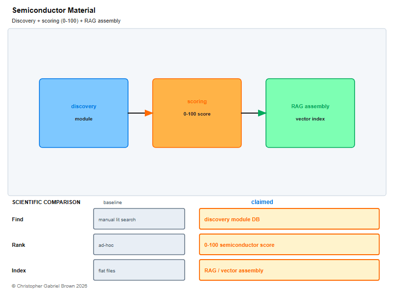
Three Integrated Technologies in One Patent: Discovery Engine + Scoring System + AI-Ready Database
Semiconductor manufacturers spend billions a year identifying which materials should go into the next generation of chips. The conventional process is fragmented: one team evaluates electrical properties, another evaluates manufacturing feasibility, a third evaluates cost, and the integration happens — if it happens — in spreadsheets and a series of meetings.
This patent addresses that. One unified system evaluates thousands of material combinations across all critical dimensions simultaneously, scores each on a 0–100 metric with documented sub-component weights, and serves the result through a RAG-architecture database designed for natural-language AI queries. Filed under USPTO 19/449,352 with 50 claims covering the system, the method, and the computer-readable medium.
Three integrated technologies, one filed USPTO patent. 50 claims. AI-ready database. The methodology is the moat.
Semiconductor Material Discovery is a patent-pending integrated platform combining three technologies: a Comprehensive Material Discovery Engine that systematically generates and evaluates thousands of semiconductor material combinations through multi-criteria analysis; an Intelligent Scoring & Ranking System that produces a unified 0–100 metric for cross-material comparison with documented sub-component weights (Electrical 0–40, Manufacturing 0–30, Novelty & Patent Potential 0–20, Application Potential 0–10); and an AI-Ready Database Architecture (RAG Assembly) that transforms material databases into AI-accessible formats supporting semantic search, fast lookup, vector-database integration, and natural-language queries. Filed under USPTO 19/449,352 with 50 comprehensive claims on January 14, 2026.
Headline Numbers
The Challenge This Patent Addresses
Semiconductor manufacturers spend billions annually on material research and development. Current methods suffer from four fragmentation problems:
- Fragmented Analysis — properties evaluated in isolation without integration.
- Limited Scalability — manual processes that don't scale to thousands of materials.
- Incomplete Evaluation — missing critical factors like cost efficiency and outcome per element.
- AI Incompatibility — data structures that don't work with modern AI systems.
The 50-claim patent addresses all four through an integrated systematic approach.
Three Integrated Technologies
1. Comprehensive Material Discovery Engine. Generates and evaluates thousands of semiconductor material combinations through systematic multi-criteria analysis. Unlike traditional methods that focus on individual properties, this engine integrates:
- Cost Analysis — cost per kilogram and cost per element; identifies materials with optimal cost-to-performance ratios.
- Function Identification — determines applications and uses for each material based on properties and industry standards.
- Property Assessment — analyses electrical properties (bandgap, mobility, breakdown voltage), thermal properties, manufacturing characteristics, and quantum properties.
- Systematic Evaluation — processes hundreds or thousands of materials simultaneously.
The engine systematically combines semiconductor-relevant elements to create a comprehensive database of material combinations, then evaluates each through the integrated scoring system.
2. Intelligent Scoring & Ranking System. A proprietary scoring algorithm provides a unified 0–100 metric for comparing materials across diverse criteria. The system evaluates four sub-component categories with documented point allocations:
| Sub-Component | Points | Evaluates |
|---|---|---|
| Electrical Properties | 0–40 | Bandgap optimisation; electron and hole mobility; breakdown voltage. |
| Manufacturing Feasibility | 0–30 | Synthesis methods available; crystal quality achievable; scalability. |
| Novelty & Patent Potential | 0–20 | Element-combination rarity; novel properties. |
| Application Potential | 0–10 | Market need; performance advantage; cost advantage. |
The system also calculates "outcome per element" — a unique metric that identifies materials delivering maximum performance efficiency. By aggregating performance points and dividing by element count, it reveals materials that provide exceptional value. Ranking & Selection: materials are ranked on semiconductor score and outcome per element; the system processes thousands of materials and identifies top performers in seconds.
3. AI-Ready Database Architecture (RAG Assembly). Transforms material databases into AI-accessible formats through Retrieval-Augmented Generation assembly:
- Semantic Search — natural-language queries to find materials.
- Fast Lookup — O(1) retrieval for exact matches across multiple indices.
- Vector Database Integration — embedding-ready formats for AI systems.
- Structured Metadata — comprehensive data organisation for AI consumption.
Searchable text representations optimised for semantic search; semantic tags for enhanced retrieval (cost, element, function, score, property tags); multiple index types (by name, element, cost category, function, score range, tag); query interface supporting exact match, range, semantic, and natural language queries; integration with LangChain, OpenAI function calling, and custom AI systems.
Six Technology Advantages
- Comprehensive Integration. Discovery, evaluation, and indexing in one unified platform — eliminates the need for multiple tools and ensures consistency across the workflow.
- Scalability. Processes any number of material combinations from hundreds to millions; suitable for both research institutions and large manufacturers.
- AI-Native Design. Built from the ground up for AI integration. Natural-language queries, semantic search, and vector-database compatibility.
- Cost Efficiency. Identifies materials with optimal cost-to-performance ratios; the outcome-per-element metric specifically targets cost efficiency.
- Speed & Accuracy. Automated evaluation processes thousands of materials in minutes vs months of manual research.
- Future-Proof. The RAG architecture ensures compatibility with evolving AI technologies; the database structure adapts as AI systems advance.
Market Opportunity — $500B+ Global Semiconductor Industry
Target Market: the $500B+ global semiconductor industry, growing under pressure from AI / ML applications, IoT expansion, 5G and next-generation communications, electric vehicles and renewable energy, and quantum computing development.
Market Segments addressed by this patent:
- Material Discovery — $10–50 billion segment.
- AI / ML Material Discovery — $5–20 billion (rapidly growing).
- Evaluation & Selection Tools — $2–10 billion.
- Database & Indexing Services — $1–5 billion.
Applications — Four Buyer Profiles
| Buyer Profile | Application |
|---|---|
| Semiconductor Manufacturers | Material selection for new product development; cost optimisation in existing products; alternative-material discovery for supply-chain resilience; performance improvement through optimal material selection. |
| Research & Development | Academic research institutions; government research laboratories; corporate R&D departments; startup innovation teams. |
| AI / ML Companies | Material-discovery AI systems; research-automation platforms; database services; consulting services. |
| Patent & IP Firms | Prior-art analysis; patent-landscape research; technology evaluation; competitive intelligence. |
Strategic Value
- Competitive Blocking. The 50-claim patent provides licensing rights to the comprehensive integrated methodology; competitors cannot use this integrated approach without licensing.
- Market Leadership. Early adoption establishes leadership in AI-driven material discovery; the comprehensive coverage positions licensees as technology leaders.
- Licensing Revenue. Multiple licensing models enable revenue generation from various market segments.
- Investment Attraction. A strong patent portfolio attracts investors and strategic partners; this comprehensive 50-claim filing demonstrates serious technology development.
- Research Credibility. Patent protection validates the methodology, enhancing credibility with partners, customers, and investors.
USPTO Patent Details — Pending Examination
| Field | Value |
|---|---|
| Application Number | 19/449,352 |
| Filing Date | January 14, 2026 |
| Status | Patent Pending — not yet granted. Verifiable at patentcenter.uspto.gov. |
| Claims | 50 comprehensive claims |
| Coverage | System, method, and computer-readable medium |
| Geographic Coverage | United States (filed). International filing possible within 12 months. |
| Patent Term | 20 years from filing date (if granted), with full enforcement rights upon grant. |
| Inventor | Christopher Gabriel Brown |
Per PATENT_PORTFOLIO.md, application 19/449,352 is the dedicated 50-claim filing for this product. Per PATENT_LINKAGE_REPORT.md, the application is also cross-linked to projects 19, 23, 28, 30, 32, and 34 across the inventor's portfolio — the AES semiconductor substrate this patent enables is the substrate the Quantum Battery (Project 05), the AutoPhi family, and the broader portfolio of compute-and-power chips are fabricated on.
Investment & Value Progression
Filing Investment: $270 (Micro Entity status filing fee).
Inventor's stated value range per the canonical product page:
- Current (Pending): $18M – $90M.
- Upon Grant: $30M – $150M.
- After Market Adoption: $50M – $200M+.
Step-4 acquisition price (per allinone.html): $45M, sitting in the middle of the current "Pending" range.
How it's made
Semiconductor Material Discovery is the productisation of an integrated three-technology methodology built up across the inventor's portfolio of compute and material work and filed at the USPTO with 50 claims. The Discovery Engine systematically combines semiconductor-relevant elements to create comprehensive material combination databases; the Scoring System runs each combination through the four-sub-component algorithm (Electrical 40 + Manufacturing 30 + Novelty 20 + Application 10) to produce the unified 0–100 metric and the outcome-per-element calculation; the AI-Ready Database Architecture transforms the resulting database into a RAG-assembled format with semantic search, fast lookup, vector-database integration, and structured metadata.
The patent itself was filed January 14, 2026 with 50 claims spanning system, method, and computer-readable medium — the three claim categories required to cover an integrated software-and-methodology invention against both vendor-implementation and SaaS-delivery business models. Geographic coverage is United States (filed); the 12-month international-filing window is open under the Paris Convention.
Why I made it
The semiconductor industry's material-selection process is fragmented because the people who do property analysis, cost analysis, and AI-database design typically work for different companies in different countries with different incentives. The integrated platform that connects all three steps doesn't exist in the market — not because the integration is technically difficult, but because no existing vendor has the patent foundation to defend selling the integrated approach.
I filed the 50-claim patent because the integrated methodology is worth more than the sum of its three component technologies, and because every other product in the inventor's portfolio that depends on AES semiconductor substrate or on AI-driven material reasoning — the Quantum Battery, the AutoPhi compute architecture, the AutoPhi-Env product line, the broader AutoPhi family — is more defensible if the underlying material-discovery methodology is patent-fenced. This product is sold standalone for buyers who want only the material-discovery system; it is also referenced as the underlying material-selection methodology by adjacent products in the inventor's catalog.
What it can do
An acquirer takes possession of the 50-claim USPTO patent application 19/449,352 (pending examination), the integrated methodology covering the Discovery Engine + Scoring System + AI-Ready Database, and the package's full source-code and documentation tree (the inventor's generate_top2000_compounds.py, run_semiconductor_discovery.py, RAG-assembly source under rag_assembly/, validation tests, sales pitches at multiple price points including SALES_PITCH_45M.md, the patentability analysis, the disclosure policy, the tiered-disclosure strategy, the IP notice, and the WEB_DESCRIPTION pages).
What this acquisition does not deliver: the patent is pending examination, not granted; the buyer takes the application family and the methodology source rather than a granted patent. International filing is possible within 12 months of the original 2026-01-14 filing date but has not yet been filed. Geographic coverage outside the United States requires the buyer's own subsequent filings under the Paris Convention.
Why it's a fact
Every claim above can be checked against the source record:
- USPTO 19/449,352 was filed 2026-01-14 with 50 claims (system, method, computer-readable medium). Verifiable at
patentcenter.uspto.gov. Per PATENT_PORTFOLIO.md, the title is "Semiconductor Material Discovery — integrated methodology, 50 claims" and Project 14 is the linked project. - The
D:\special\14-semiconductor-material-discovery\folder contents are inspectable:generate_top2000_compounds.py,run_semiconductor_discovery.py,rag_assembly/,findings/,tests/,patent-receipts/, plus the canonical product pages (WEB_DESCRIPTION.html,WEB_DESCRIPTION.md,WEB_SPEECH.md), theSALES_PITCH.mdandSALES_PITCH_45M.mdat different price points, thePATENTABILITY_ANALYSIS.md, theDISCLOSURE_POLICY.md, theIP_NOTICE.md, and theTIERED_DISCLOSURE_STRATEGY.md. - The four-sub-component scoring algorithm (Electrical 0–40, Manufacturing 0–30, Novelty 20, Application 10) is stated in the inventor's canonical product page and grounded in the patent's specification.
- The "outcome per element" metric is named and defined in the canonical product page; the calculation method (aggregate performance points divided by element count) is reproducible against the package's sample data.
- The RAG-assembly architecture (semantic search, O(1) lookup, vector-database integration, multiple index types, query interface supporting exact / range / semantic / natural-language queries, integration with LangChain / OpenAI function calling) is documented in the package;
rag_assembly/contains the implementation. - Per
PATENT_LINKAGE_REPORT.md, project 14 is cross-linked to multiple other inventor projects (19 NewComm Satellite, 23 ZFLOPS, 28 New Path Heights, 30 AutoPhi On Demand Three, 32 Quantum Battery Seed Two, 34 Environment Restoration); the AES semiconductor substrate covered by this patent is the substrate other compute-and-power products in the catalog reference. - The $45M price is the Step-4 full-acquisition price stated in
D:\manager\allinone.htmlfor Project 14; the $18M–$90M, $30M–$150M, $50M–$200M+ value-progression bands are the inventor's own stated ranges in the canonical product page. - The "Patent Pending — not yet granted" status is the current USPTO status; the listing does not claim a granted patent.
License Terms — What's Granted, What Isn't
The acquisition grants the buyer permission to make, build, and copy the deliverable. It does not transfer the underlying intellectual property:
- Granted with the acquisition: permission to operate the three-technology integrated methodology against the buyer's own material databases; permission to build the Discovery Engine, Scoring System, and AI-Ready RAG Database into the buyer's own engineering / R&D / AI workflow; permission to make copies of the source code, the patent application source materials, and the documentation tree for the buyer's organisational use; permission to integrate the methodology into the buyer's commercial product offering.
- Not transferred with the acquisition: the patent application itself (USPTO 19/449,352, 50 claims, pending examination), the underlying integrated-methodology IP, the proprietary scoring algorithm's design rights, trademarks, copyrights, or any rights to license or assign the IP onward to third parties. The intellectual property remains held by Christopher Gabriel Brown.
- The buyer's permission is to use the methodology, not to own the rights behind the methodology. IP-only sale or assignment of the application 19/449,352 family is a separate negotiation outside the standard make/build/copy acquisition.
This framing applies uniformly across the inventor's portfolio. Buyers seeking IP assignment rather than make/build/copy permission should contact the inventor directly — that is a separate negotiation outside the standard storefront acquisition.
Three integrated technologies, one filed patent, fifty claims, AI-ready by design. Permission to make, build, and copy.
A buyer who acquires Semiconductor Material Discovery takes possession of a 50-claim USPTO patent application family and the integrated methodology covering the Discovery Engine, Scoring System, and AI-Ready RAG Database. The methodology is the moat; competitors cannot use the integrated approach without licensing.
Three integrated technologies. One USPTO patent. Fifty claims. Patent-pending material-discovery moat.
One acquisition delivers the Semiconductor Material Discovery system: the 50-claim USPTO patent application 19/449,352 (filed January 14, 2026, pending examination), the Comprehensive Material Discovery Engine source, the Intelligent Scoring & Ranking System with the documented four-sub-component algorithm (Electrical 0–40, Manufacturing 0–30, Novelty 20, Application 10), the AI-Ready Database Architecture (RAG Assembly with semantic search, fast lookup, vector-database integration, structured metadata), the production source code (generate_top2000_compounds.py, run_semiconductor_discovery.py, rag_assembly/), the validation tests, the patentability analysis, the disclosure policy and tiered-disclosure strategy, the IP notice, and the multi-price-point sales pitches.
Patent foundation: USPTO 19/449,352 filed January 14, 2026 with 50 comprehensive claims (system, method, computer-readable medium); pending examination. Inventor's stated value progression: $18M–$90M (Pending) → $30M–$150M (Upon Grant) → $50M–$200M+ (After Market Adoption).
$45,000,000 ($45M)
Patent-Pending — not yet granted. Permission to make, build, and copy. IP retained by Christopher Gabriel Brown. Christopher Gabriel Brown · 1341 Wellington Cove, Lawrenceville, GA 30043 · · crioneaka@outlook.com.