
AutoPhi 1536 Escape Interposer - Access (12-layer, 506/960)
Complete escape-routing interposer for the AutoPhi ball-out — the cheapest path to a fan-out project without hand-solving the routing. Skip the interposer design cycle.
Why this is worth what it costs
Reusing a proven library means your engineering hours go into differentiation, not re-solving problems CRI-ONE already solved. What you are paying for is 15+ years of AutoPhi R&D, publicly documented since 2010 and patent-filed since 2012 — packaged as a frozen v1 you can drop into your design flow.
What ships in the license
All files needed to bring this asset into your design flow — source, layouts, netlists where applicable, and the corresponding foundry / EDA documentation. Delivered as an AES-256 encrypted downloadable archive.
What you own after the sale
The right to use, modify, and integrate this asset into your own products.
Derivative rights to spin variants without coming back to CRI-ONE.
Exclusive license for this implementation. No one else can ship this specific asset while you hold the license.
Priority-date defense
The foundational AutoPhi architecture is publicly documented from 2010 (Internet Archive) and patent-filed from 2012 (USPTO), under CRI-ONE’s name and independently verifiable. No prior art can invalidate the claims that come with your license.
© CRI-ONE. All rights reserved. Patents issued and pending. Unauthorized reproduction of the underlying designs is prohibited.
Extended catalog & full narrative — AutoPhi 1536 Escape Interposer - Access (12-layer, 506/960)
The extended dossier appended from the 2026-08-05 catalog snapshot. Prices in the body copy have been stripped; the live-store price on this page is the authoritative figure. Images have been omitted.
A 48 × 32 die footprint at 0.8 mm pitch, fanned out to the same array at 2.0 mm. 2.5× escape on a 12-layer substrate, fully routed and DRC-checked. Editable KiCad source.
What this is
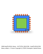
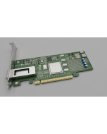
An escape interposer. It solves one problem and solves it completely: you have a die on a fine pad grid and a board that cannot be built to that pitch. This substrate sits between them. Fine side is 1,536 pads on a 0.8 mm grid across 37.6 × 24.8 mm. Coarse side is the same 48 × 32 array on a 2.0 mm grid across 94.0 × 62.0 mm.
That pitch change is the entire value. A 2 mm BGA is an ordinary board with ordinary design rules and ordinary yield. The fine-pitch escape, which is the part that needs HDI process and a routing strategy that does not run out of layers, is done here and does not have to be solved again downstream.
This is a blueprint, not a board. You receive the design files. You have it fabricated.
The substrate at a glance
| Property | Value |
| Outline | 95.1 x 90.1 mm |
| Copper layers | 12 |
| Fine side (die) | 1,536 pads, 48 x 32, 0.8 mm pitch, 0.35 mm pads |
| Coarse side (BGA) | 1,536 pads, 48 x 32, 2.0 mm pitch, 0.9 mm pads |
| Fan-out ratio | 2.5x |
| Signal balls | 960 |
| Power / ground balls | 576 on 1V0, APH_VDD_CORE, GND |
| Nets | 891 |
| Tracks | 1,755 |
| Vias | 960 blind, 1,536 microvia |
| Escape routed | 506 of 960 signal balls |
Layer stackup
Signal layers carry the escape. Plane layers are solid pours that the rail balls drop straight into, which is why 576 of the 1,536 balls never consume a routing channel at all.
| # | Layer | Type |
| 1 | TOP | signal |
| 2 | GND1 | plane |
| 3 | SIG1 | signal |
| 4 | SIG2 | signal |
| 5 | PWR1 | plane |
| 6 | SIG3 | signal |
| 7 | SIG4 | signal |
| 8 | PWR2 | plane |
| 9 | SIG5 | signal |
| 10 | SIG6 | signal |
| 11 | GND2 | plane |
| 12 | BOTTOM | signal |
Routing, layer by layer
| Layer | Track segments |
| BOTTOM | 92 |
| SIG1 | 343 |
| SIG2 | 267 |
| SIG3 | 251 |
| SIG4 | 274 |
| SIG5 | 259 |
| SIG6 | 269 |
Design rules
| Constraint | Value |
| Minimum track width | 0.075 mm |
| Minimum clearance | 0.075 mm |
| Minimum via diameter | 0.2 mm |
| Minimum via annular ring | 0.1 mm |
| Minimum microvia diameter | 0.2 mm |
| Minimum microvia drill | 0.1 mm |
| Minimum hole clearance | 0.25 mm |
| Minimum hole to hole | 0.25 mm |
| Copper to board edge | 0.5 mm |
These are HDI numbers. Laser-drilled microvias, blind vias and via-in-pad are all used. Confirm your fabricator quotes this process before ordering — it is not a standard two-week prototype stackup.
What is in the download
- The routed
.kicad_pcbsubstrate, editable - KiCad project with the full net class and stackup setup
- Die and BGA footprints, both grids, with pin maps
- Fabrication package: gerbers, Excellon drill, drill map and report, IPC-2581, and a stackup README
- 3D models and the exported STEP of the assembled substrate
What is done and what is not
The escape is routed for 506 of 960 signal balls. Rail balls drop directly to the plane layers through their own vias and are complete. Copper pours on the signal layers are not placed — the planes are poured, the signal layers are not, which is normal for a substrate of this kind but worth knowing before you quote it.
The board carries pre-existing DRC entries unrelated to the escape: annular ring and via diameter warnings against the strictest netclass, and copper-to-edge entries around the outline. They are documented in KNOWN-ISSUES.txt in the package with the count and the cause for each. Nothing is hidden and nothing is described as clean that is not.
Who this is for
Anyone landing a fine-pitch die on a board that cannot hold fine pitch, and anyone who wants to read a complete, working answer to the BGA escape problem rather than derive one. The routing strategy, the layer assignment and the via spans are all visible and editable.
2ab235cf5fe87107095484d848b321c66f763454e121931cc8168d1cb7e41578
AutoPhi 1536 Escape Interposer - Access (12-layer, 506/960)
Publicly online since 2010 · U.S. patent applications since 2012 · inventions offered since 2014. The work of Christopher Gabriel Brown, independently documented.