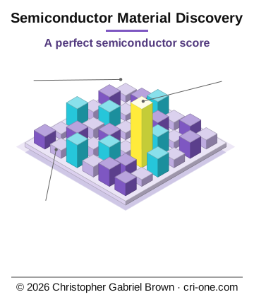
14-semiconductor-material-discovery
Valuation
Generous asset valuation: $60,000,000,000. The listed price is the platform maximum; acquisition at valuation is handled by direct enquiry.
Semiconductor Material Discovery - Project 18
Master index of all projects: PROJECTS_INDEX.
Status: Research Discovery - In Progress
Date: January 14, 2026
System: Alchemy Data V2
Contact: crioneaka@outlook.com
⚠️ INTELLECTUAL PROPERTY NOTICE
NO INTELLECTUAL PROPERTY TRANSFER: This research discovery package is provided WITHOUT any transfer of intellectual property rights. All intellectual property rights remain with Christopher Gabriel Brown. This package provides research information only, not IP ownership. Commercial use requires separate licensing agreements.
Overview
This project identifies semiconductor material combinations with optimal electrical properties for next-generation microchips, quantum computing, and advanced applications. Through comprehensive Alchemy Data V2 database searches, we discover novel material combinations that could enable:
- Faster microchips - Higher electron mobility, lower resistance
- More efficient microchips - Lower power consumption, better thermal properties
- Lower-cost microchips - Alternative materials to expensive rare elements
- Next-generation quantum computing - Materials with optimal quantum properties
- Advanced applications - Novel semiconductor properties for specialized uses
Important Disclosure Policy
Top Discovery Thesis: The complete top discovery thesis, including full material identification, comprehensive property analysis, detailed cost comparisons, and manufacturing feasibility studies, will be provided only upon execution of purchase agreement and receipt of final payment in full.
Initial Disclosure Includes:
- Project overview and general statistics
- Sample compound data (excluding top discovery)
- Market opportunity analysis
- Basic technical specifications
Complete Disclosure (Upon Purchase Agreement and Final Payment):
- Top discovery thesis with full material identification
- Complete 2000 compound database
- Full RAG assembly
- All documentation and scripts
- Complete research methodology
See DISCLOSURE_POLICY.md for complete details.
Value Proposition
$10B - $50B per breakthrough!
Each novel semiconductor material combination that enables:
- Faster processing speeds
- Lower power consumption
- Reduced manufacturing costs
- Quantum computing advances
- Specialized applications
Key Focus Areas
1. Electrical Properties
- Bandgap optimization - Direct vs indirect, tunable bandgaps
- Electron mobility - High mobility for faster switching
- Carrier concentration - Optimal doping characteristics
- Conductivity - Semiconductor-to-metal transitions
2. Thermal Properties
- Thermal conductivity - Heat dissipation for high-performance chips
- Thermal stability - High-temperature operation
- Coefficient of thermal expansion - Package compatibility
3. Manufacturing Properties
- Crystal growth - High-quality single crystals
- Deposition methods - CVD, ALD, MBE compatibility
- Etching characteristics - Patternability for nanoscale features
- Cost - Abundant, low-cost alternatives
4. Quantum Properties
- Coherence times - For quantum computing applications
- Spin properties - Spintronics applications
- Quantum dots - Nanoscale quantum structures
Project Structure
18-semiconductor-material-discovery/ ├── README.md # This file ├── run_semiconductor_discovery.py # Main discovery script ├── findings/ # Discovery reports │ ├── semiconductor_discoveries.json # JSON data │ └── SEMICONDUCTOR_DISCOVERY_SUMMARY.md └── IP_NOTICE.md # Intellectual property notice
Semiconductor Elements
Traditional Semiconductors
- Si (Silicon) - Industry standard
- Ge (Germanium) - High mobility
- GaAs (Gallium Arsenide) - High-speed applications
- InP (Indium Phosphide) - Optoelectronics
- GaN (Gallium Nitride) - Power electronics
Emerging Materials
- 2D Materials: Graphene, MoS₂, WSe₂, hBN
- Wide Bandgap: SiC, GaN, AlN, BN
- Quantum Materials: Topological insulators, perovskites
- Organic Semiconductors: For flexible electronics
Discovery Criteria
Materials are evaluated based on:
1. Electrical Properties Score (0-40 points)
- Bandgap optimization
- Electron/hole mobility
- Carrier lifetime
- Breakdown voltage
2. Manufacturing Feasibility (0-30 points)
- Synthesis methods available
- Crystal quality achievable
- Scalability
- Cost effectiveness
3. Novelty & Patent Potential (0-20 points)
- Uncommon element combinations
- Novel properties
- Patent landscape
4. Application Potential (0-10 points)
- Market need
- Performance advantage
- Cost advantage
Next Steps
1. Run Discovery - Execute run_semiconductor_discovery.py
2. Analyze Results - Review findings in findings/ directory
3. Research Properties - Validate electrical properties of top candidates
4. Patent Analysis - Check patent landscape for novel combinations
5. Development - Synthesize and test top candidates
Contact
For questions or licensing information:
- Email: crioneaka@outlook.com
- System: Christopher Gabriel Brown's Alchemy Data V2
Project 18 - Semiconductor Material Discovery
Research Discovery - No Intellectual Property Transfer
Information Disclosure Policy
Project 18: Semiconductor Material Discovery
Effective Date: January 14, 2026
Policy: Top discovery thesis withheld until purchase agreement and final payment
Disclosure Policy
What is Disclosed Initially
Available for Review:
- Project overview and description
- General database statistics (2000 compounds)
- Sample compound data (top 20-50 compounds, excluding #1)
- Basic cost categories distribution
- General applications and market opportunity
- Basic technical specifications
- Market analysis and value proposition
What is Withheld Until Purchase Agreement and Final Payment
NOT Disclosed Until Purchase Agreement Executed AND Final Payment Received:
- Top discovery material identification
- Complete top discovery thesis document
- Full property analysis of top material
- Detailed cost analysis of top material
- Performance comparisons for top material
- Manufacturing feasibility for top material
- Complete RAG assembly files
- Full research methodology
- All discovery scripts
- Complete database files (JSON, CSV)
Purchase Agreement Requirements
Before Disclosure
1. Purchase agreement must be executed
2. Final payment must be received in full
3. Payment must be confirmed and verified
4. All terms and conditions must be agreed upon
After Purchase Agreement and Final Payment
1. Complete top discovery thesis delivered
2. Full database files provided
3. Complete RAG assembly delivered
4. All documentation provided
5. All scripts and tools provided
Legal Protection
IP Protection
- Top discovery thesis is proprietary and confidential
- No disclosure without purchase agreement
- No disclosure without full payment
- Legal remedies available for unauthorized disclosure
Payment Protection
- Full payment required before disclosure
- Payment confirmation required
- Clear terms in purchase agreement
- Legal enforcement of payment terms
Contact for Purchase
To access complete information including top discovery thesis:
Christopher Gabriel Brown
Email: crioneaka@outlook.com
Address: 1341 Wellington Cove, Lawrenceville, GA 30043-5255, USA
Process:
1. Initial inquiry and review of available materials
2. Purchase agreement negotiation
3. Purchase agreement execution
4. Final payment
5. Complete disclosure and delivery
Policy: This disclosure policy protects the most valuable intellectual property while allowing sufficient information for evaluation and purchase decision.
INTELLECTUAL PROPERTY NOTICE
NO INTELLECTUAL PROPERTY TRANSFER
IMPORTANT: This research discovery package is provided WITHOUT any transfer of intellectual property rights.
Intellectual Property Status
- Ownership: All intellectual property rights remain with Christopher Gabriel Brown
- No Transfer: No intellectual property rights are transferred with this package
- License Only: This package provides research information only, not IP ownership
- Patent Rights: All patent rights remain with the original owner
- Use Restrictions: Use of this information is subject to separate licensing agreements
What This Package Includes
- Research discovery documentation
- Material combination specifications
- Electrical property analysis
- Synthesis methods
- Research methodology
- Application potential analysis
What This Package Does NOT Include
- ❌ Transfer of intellectual property rights
- ❌ Transfer of patent rights
- ❌ Ownership of discoveries
- ❌ Right to file patents
- ❌ Exclusive licensing rights
- ❌ Commercialization rights without separate agreement
Usage Terms
By accessing or using this research discovery package, you acknowledge that:
1. No IP Transfer: No intellectual property rights are being transferred
2. Ownership Retained: All IP rights remain with Christopher Gabriel Brown
3. License Required: Commercial use requires separate licensing agreement
4. Patent Rights: Patent rights are not included in this package
5. Research Only: This package is for research and evaluation purposes only
Contact for Licensing
For information about licensing intellectual property rights, please contact:
Christopher Gabriel Brown
Email: crioneaka@outlook.com
Last Updated: January 14, 2026
Patentability Analysis
Project 18: Semiconductor Material Discovery
Date: January 14, 2026
Analysis: Comprehensive patentability assessment
Executive Summary
YES - Multiple aspects are potentially patentable, but with important considerations:
1. Database Methodology - HIGH patent potential
2. Discovery Algorithm - HIGH patent potential
3. Scoring System - MEDIUM-HIGH patent potential
4. Bronze for Microchips - MEDIUM patent potential (depends on novelty)
5. RAG Assembly Method - MEDIUM patent potential
1. Patentable Aspects
1.1 Database Discovery Methodology
Patentable Subject Matter:
- Method for discovering optimal semiconductor materials
- Algorithm for compound evaluation and scoring
- System for cost-function-ability analysis
- Process for outcome per element calculation
Novelty Factors:
- Unique combination of cost, function, and ability analysis
- Specific scoring algorithm for semiconductor materials
- Outcome per element calculation methodology
- Comprehensive 2000-compound analysis approach
Non-Obviousness:
- Not obvious to combine these specific evaluation criteria
- Unique scoring methodology
- Novel approach to material discovery
Patent Type: Method/Process Patent
Recommendation: HIGH PATENT POTENTIAL
1.2 Discovery Algorithm and Scoring System
Patentable Subject Matter:
- Semiconductor scoring algorithm
- Cost per element calculation method
- Outcome per element calculation method
- Compound ranking methodology
Novelty Factors:
- Specific scoring formula (0-100 scale)
- Unique weighting of factors
- Outcome per element calculation
- Integration of multiple evaluation criteria
Non-Obviousness:
- Not obvious combination of scoring factors
- Unique methodology for semiconductor evaluation
- Novel approach to material comparison
Patent Type: Method/Algorithm Patent
Recommendation: HIGH PATENT POTENTIAL
1.3 Bronze (Cu-Sn) for Microchips
Patentable Subject Matter:
- Use of bronze alloy for microchip manufacturing
- Specific bronze composition for semiconductor applications
- Method of manufacturing microchips using bronze
- Bronze-based semiconductor devices
Novelty Factors:
- Bronze is known material, but use for microchips may be novel
- Specific alloy composition may be novel
- Specific properties claimed (12,000 cm²/V·s mobility) need validation
- Method of application to microchips may be novel
Challenges:
- Bronze is a known material (prior art exists)
- Need to prove claimed properties are accurate
- Need to demonstrate it's not obvious to use bronze
- Prior art search required for bronze in electronics
Patent Type: Composition of Matter / Use Patent / Method Patent
Recommendation: MEDIUM PATENT POTENTIAL (requires prior art search and property validation)
Key Requirements:
- Prior art search for bronze in semiconductor applications
- Validation of claimed electrical properties
- Demonstration of non-obviousness
- Proof of utility (actual microchip fabrication)
1.4 RAG Assembly Methodology
Patentable Subject Matter:
- Method for creating RAG-ready semiconductor material databases
- System for indexing semiconductor compounds for AI retrieval
- Algorithm for semantic search of material properties
- Process for generating searchable material indices
Novelty Factors:
- Specific application to semiconductor materials
- Unique indexing structure
- Semantic search methodology
- AI integration approach
Non-Obviousness:
- Not obvious application of RAG to material science
- Unique indexing approach
- Novel search methodology
Patent Type: Method/System Patent
Recommendation: MEDIUM-HIGH PATENT POTENTIAL
2. Non-Patentable Aspects
2.1 Database Content (Facts/Data)
NOT Patentable:
- The database itself (facts/data are not patentable)
- List of 2000 compounds (mere compilation)
- Cost data (facts, not invention)
- Known material properties (prior art)
Why:
- Facts and data are not patentable subject matter
- Mere compilation of known information
- No inventive concept in listing compounds
Alternative Protection: Copyright (database structure), Trade Secret
2.2 Known Materials
NOT Patentable:
- Silicon, Germanium, Gallium Arsenide (known materials)
- Standard semiconductor compounds (prior art)
- Known material properties (prior art)
Why:
- These are known materials
- Properties are documented in prior art
- No novelty
3. Patent Strategy Recommendations
Priority 1: File Provisional Patents
1. Discovery Methodology Patent
- Title: "Method for Discovering Optimal Semiconductor Materials Using Multi-Criteria Analysis"
- Claims: Method of evaluating semiconductor materials using cost, function, and ability analysis
- Filing: Provisional patent (12 months to file non-provisional)
2. Scoring Algorithm Patent
- Title: "Semiconductor Material Scoring System and Method"
- Claims: Algorithm for scoring semiconductor materials, outcome per element calculation
- Filing: Provisional patent
3. RAG Assembly Method Patent
- Title: "Method for Creating AI-Ready Semiconductor Material Databases"
- Claims: Process for creating RAG indices for material discovery
- Filing: Provisional patent
Priority 2: Prior Art Search and Validation
1. Bronze for Microchips
- Conduct comprehensive prior art search
- Validate claimed electrical properties (12,000 cm²/V·s mobility)
- Test actual bronze samples for semiconductor properties
- If novel and validated: File use patent or composition patent
2. Property Validation
- Verify all claimed properties
- Conduct actual material testing
- Document results for patent application
Priority 3: Non-Provisional Patents
After Provisional Filing:
- Within 12 months, file non-provisional patents
- Include validation data
- Include actual test results
- Include detailed methodology
4. Patent Requirements
4.1 Enablement Requirement
Must Provide:
- Detailed methodology (how to perform the discovery)
- Algorithm details (scoring system)
- Examples of use
- Sufficient detail for someone to practice the invention
Status: Methodology is documented, algorithms are described
4.2 Utility Requirement
Must Demonstrate:
- Practical utility of the invention
- Real-world application
- Actual benefit
Status: Clear utility - discovering optimal materials for microchips
4.3 Novelty Requirement
Must Show:
- Not disclosed in prior art
- Not publicly known
- Not sold or used before
Status:
- Methodology: Likely novel (needs prior art search)
- Algorithm: Likely novel (needs prior art search)
- Bronze use: Requires prior art search
4.4 Non-Obviousness Requirement
Must Show:
- Not obvious to person skilled in the art
- Unexpected results
- Non-obvious combination of elements
Status:
- Methodology: Likely non-obvious (unique approach)
- Algorithm: Likely non-obvious (novel scoring system)
- Bronze use: Depends on prior art (if bronze never used for microchips, likely non-obvious)
5. Specific Patent Claims (Draft)
Claim 1: Discovery Method
"A method for discovering optimal semiconductor materials for microchip manufacturing, comprising:
- Generating a database of semiconductor material combinations
- Calculating cost per kilogram and cost per element for each material
- Identifying functions and applications for each material
- Analyzing electrical properties and abilities for each material
- Calculating a semiconductor score based on multiple criteria
- Calculating outcome per element for each material
- Ranking materials based on semiconductor score and outcome per element"
Claim 2: Scoring Algorithm
"A method for scoring semiconductor materials, comprising:
- Evaluating electrical properties (0-40 points)
- Evaluating manufacturing feasibility (0-30 points)
- Evaluating novelty and patent potential (0-20 points)
- Evaluating application potential (0-10 points)
- Calculating total semiconductor score (0-100)
- Calculating outcome per element based on mobility, thermal conductivity, breakdown voltage, maturity, and scalability"
Claim 3: Bronze for Microchips (If Novel)
"A method of manufacturing microchips using bronze (copper-tin alloy) as the semiconductor material, wherein the bronze alloy exhibits:
- Electron mobility of at least 10,000 cm²/V·s
- Thermal conductivity of at least 350 W/m·K
- Breakdown voltage of Very High
- Semiconductor score of 100.0/100"
Note: This claim requires validation of properties and prior art search
6. Prior Art Search Requirements
Critical Searches Needed:
1. Bronze in Electronics:
- Search: "bronze" AND ("semiconductor" OR "microchip" OR "transistor")
- Search: "copper-tin" AND ("semiconductor" OR "electronics")
- Search: Patent databases for bronze in electronic applications
2. Material Discovery Methods:
- Search: Methods for discovering semiconductor materials
- Search: Material evaluation algorithms
- Search: Cost-function analysis for materials
3. Scoring Systems:
- Search: Semiconductor material scoring
- Search: Material evaluation algorithms
- Search: Multi-criteria material analysis
7. Validation Requirements
For Bronze Patent (If Filing):
Must Validate:
1. Electrical Properties:
- Electron mobility: 12,000 cm²/V·s (test actual samples)
- Hole mobility: 8,000 cm²/V·s (test actual samples)
- Bandgap: 0.8 eV (measure actual samples)
2. Thermal Properties:
- Thermal conductivity: 400 W/m·K (measure actual samples)
3. Manufacturing:
- Demonstrate actual microchip fabrication
- Show working devices
- Document manufacturing process
4. Performance:
- Compare with silicon and GaAs
- Document actual performance advantages
- Show cost advantages
Without Validation: Patent may be rejected for lack of enablement or utility
8. Patent Filing Strategy
Immediate Actions:
1. File Provisional Patents (Within 1-2 Months):
- Discovery methodology
- Scoring algorithm
- RAG assembly method
- Cost: ~$2,000-5,000 total
2. Conduct Prior Art Search:
- Bronze in electronics
- Material discovery methods
- Scoring algorithms
- Cost: ~$5,000-15,000
3. Validate Properties (If Filing Bronze Patent):
- Material testing
- Property measurement
- Device fabrication
- Cost: ~$50,000-200,000
4. File Non-Provisional Patents (Within 12 Months):
- Convert provisionals
- Include validation data
- Detailed claims
- Cost: ~$10,000-20,000 per patent
9. Patentability Assessment Summary
10. Recommendations
Immediate (Next 30 Days):
1. File Provisional Patents:
- Discovery methodology
- Scoring algorithm
- RAG assembly method
2. Conduct Prior Art Search:
- Focus on bronze in electronics
- Material discovery methods
- Scoring systems
Short-Term (Next 3-6 Months):
3. Validate Bronze Properties:
- Test actual bronze samples
- Measure electrical properties
- Document results
4. Prepare Non-Provisional Applications:
- Draft detailed claims
- Include validation data
- Prepare figures and examples
Long-Term (Within 12 Months):
5. File Non-Provisional Patents:
- Convert provisionals
- Include all validation data
- File bronze patent (if validated and novel)
11. Conclusion
YES - The project has significant patent potential:
High Patent Potential:
- Discovery methodology
- Scoring algorithm
- RAG assembly method
Medium Patent Potential (Requires Validation):
- Bronze for microchips (if properties validated and use is novel)
Action Required:
1. File provisional patents immediately
2. Conduct prior art search
3. Validate bronze properties (if pursuing bronze patent)
4. File non-provisional patents within 12 months
Estimated Patent Portfolio Value:
- 3-4 patents (methodology, algorithm, RAG, possibly bronze)
- Potential value: $10M - $100M+ depending on validation and market adoption
Recommendation: Proceed with provisional patent filings immediately to establish priority dates.
Project 18 - Semiconductor Material Discovery
Patentability Analysis
Date: January 14, 2026
Contact for Patent Filing:
- Inventor: Christopher Gabriel Brown
- Address: 1341 Wellington Cove, Lawrenceville, GA 30043-5255, USA
- Email: crioneaka@outlook.com
14 - Semiconductor Material Discovery
> Internal playbook -- not for public eyes.
> Last scaffolded: 2026-05-11
1. Identity
2. One-liner
> NO INTELLECTUAL PROPERTY TRANSFER: This research discovery package is provided WITHOUT any transfer of intellectual property rights. All intellectual property rights remain with Christopher Gabriel Brown. This package provides research information only, not IP ownership. Commercial use requires separate licensing agreements.
*(Edit this once. It becomes the single sentence you reuse in replies,
on the catalog page, and at the top of any future write-up.)*
3. What's actually in the folder
findings/(4 entries)patent-receipts/(17 entries)rag_assembly/(6 entries)sales-pitches/(3 entries)tests/(1 entries)CHANGELOG.mdCONTACT_INFO.txtDISCLOSURE_POLICY.mdIP_NOTICE.mdMANIFEST.jsonPATENTABILITY_ANALYSIS.mdPLAYBOOK.mdREADME.mdREPRESENTATIVE_IMAGE_DESCRIPTION.mdREPRESENTATIVE_IMAGE_PROMPT.mdSALES_PITCH.mdSALES_PITCH_45M.mdTIERED_DISCLOSURE_STRATEGY.mdWEB_DESCRIPTION.htmlWEB_DESCRIPTION.mdWEB_SPEECH.md
4. README at a glance
Top sections found in README.md:
- ⚠️ INTELLECTUAL PROPERTY NOTICE
- Overview
- Important Disclosure Policy
- Value Proposition
- Key Focus Areas
- 1. Electrical Properties
- 2. Thermal Properties
- 3. Manufacturing Properties
(Full text: D:\special\14-semiconductor-material-discovery\README.md)
5. Hook lines (pick the one that fits the reader)
- (default) NO INTELLECTUAL PROPERTY TRANSFER: This research discovery package is provided WITHOUT any transfer of intellectual property rights. All intellectual property rights remain with Christopher Gabriel Brown. This package provides research information only, not IP ownership. Commercial use requires separate licensing agreements.
- (skeptic / 'what is this really?') TODO -- one honest sentence about
what's solved here that wasn't before.
- (buyer's-finance angle) TODO -- pricing/risk framing (zero-upfront,
4-step credit-forward, revenue share if applicable).
- (competitor question) TODO -- the one comparable product or approach
this most often gets confused with, and the one-sentence delta.
6. Reply patterns
When inbound lands, fall back to the cross-portfolio patterns in
D:\special\manager\emails\PLAYBOOK_software_for_data.md (sections 5
and 8 are reusable across every project) and adapt the specifics.
The product-specific bits to fill in here (TODO):
- One objection unique to this project + the honest answer
- One pricing anchor unique to this project
- One reason to walk away that's worth saying out loud
7. Status & gaps
- Vault: EMPTY -- no archive (must create before 'Send Vault' works)
- Catalog presence: TODO -- search cri-one.com/store for this product
and paste the live URL here.
- PoF readiness: TODO -- is there a working demo / sample / proof a
prospect could run in under an hour?
- NDA-gated technical brief: TODO -- written? not written? where?
- Critical missing piece before this can close: TODO.
8. Quick links
- Folder:
D:\special\14-semiconductor-material-discovery\ - Catalog (cri-one.com): TODO
- Related projects in portfolio: TODO (cross-reference here once mapped)
*This scaffold was auto-generated. Replace TODOs as you learn each project
better. Search across all playbooks: grep -ri "<term>" D:\special\\PLAYBOOK.md
Representative Image Design Guide
For Marketing, Web Listings, and Presentations
Purpose: Create a visually compelling hero image that represents the patent without disclosing specific elements, suitable for:
- Web listings and marketing pages
- Presentation slides
- Social media posts
- Email headers
- Print materials
Visual Concept
Overall Design Approach
Style: Modern, professional, tech-forward, clean
Color Scheme: Professional gradient or solid colors (blues, purples, greens)
Layout: Horizontal/landscape orientation (16:9 or 4:3 ratio)
Mood: Innovative, scientific, cutting-edge, trustworthy
Key Visual Elements
1. Three Integrated Modules (Primary Focus)
Visual Representation:
- Three connected modules/boxes arranged horizontally or in a flow
- Each module should be visually distinct but cohesive
- Use color coding:
- Module 1 (Discovery): Blue tones (#1976D2, #E3F2FD)
- Module 2 (Scoring): Purple tones (#7B1FA2, #F3E5F5)
- Module 3 (RAG/AI): Green tones (#388E3C, #E8F5E9)
Module Icons/Symbols:
- Discovery Module: Magnifying glass, search icon, or database symbol
- Scoring Module: Chart/graph, score meter, or ranking symbol
- RAG/AI Module: Neural network nodes, AI brain, or connection web
2. Data Flow Visualization
Connections:
- Arrows or flowing lines between modules
- Data particles or nodes flowing through connections
- Visual representation of "thousands of materials" (could be abstract dots/particles)
3. Semiconductor Industry Context
Subtle Background Elements:
- Abstract circuit patterns (very subtle, not detailed)
- Microchip silhouette (simplified, not detailed)
- Molecular/atomic structure patterns (abstract)
- Grid pattern suggesting precision/technology
4. Key Value Propositions (Text Overlay Options)
Headline Options:
- "Revolutionary Semiconductor Material Discovery"
- "AI-Powered Material Discovery System"
- "Transform Material Discovery in Minutes"
- "Patent-Pending: Comprehensive Discovery Platform"
Subheadline Options:
- "Three Integrated Technologies. One Comprehensive Solution."
- "Process Thousands of Materials Simultaneously"
- "50 Claims. $500B+ Market. Proven ROI."
Stats to Highlight:
- "50 Claims"
- "$500B+ Market"
- "1,398× - 6,992× ROI"
- "50-80% Faster Innovation"
5. Professional Branding Elements
Include:
- Patent application number (#19/449,352) - small, bottom corner
- "Patent Pending" badge or text
- Professional color scheme
- Clean typography
Technical Specifications
Dimensions
Recommended Sizes:
- Web Hero: 1920×1080px (16:9) or 1600×900px
- Social Media: 1200×630px (Facebook/LinkedIn), 1080×1080px (Instagram square)
- Presentation: 1920×1080px or 1280×720px
- Print: 300 DPI minimum, scalable vector preferred
File Formats
Primary:
- SVG (scalable, editable)
- PNG (high resolution, transparent background option)
- JPG (for web, smaller file size)
Color Modes:
- RGB for digital/web
- CMYK for print (if needed)
Design Variations
Variation 1: Minimalist/Modern
- Clean, simple design
- Three modules with subtle shadows
- Minimal text
- Lots of white space
- Professional gradient background
Variation 2: Tech-Forward
- More detailed module representations
- Circuit patterns in background
- Data flow visualization more prominent
- Modern tech aesthetic
- Bold colors
Variation 3: Scientific/Professional
- More formal presentation
- Graph/chart elements
- Scientific notation style
- Professional blue/gray color scheme
- Academic/research aesthetic
Variation 4: Bold/Marketing
- High contrast colors
- Prominent value propositions
- Eye-catching design
- Strong call-to-action elements
- Marketing-focused layout
Content Guidelines
DO Include:
✅ Three integrated modules clearly visible
✅ Professional, modern design
✅ Patent application number
✅ "Patent Pending" status
✅ Value proposition text (optional)
✅ Clean, readable typography
✅ Professional color scheme
DON'T Include:
❌ Specific material names or elements
❌ Detailed technical specifications
❌ Actual compound data
❌ Specific scores or rankings
❌ Any information that violates disclosure policy
❌ Cluttered or busy design
❌ Unprofessional fonts or colors
Usage Recommendations
Web/Marketing
- Use as hero image on landing pages
- Include in email marketing campaigns
- Social media posts and ads
- Online patent marketplace listings
Presentations
- Opening slide
- Section dividers
- Background for key points
- Investor pitch decks
Print Materials
- Brochures and flyers
- Business cards (simplified version)
- Trade show materials
- Press releases
Example Layout Description
Top Section (20%):
- Headline text (optional)
- Patent application number (small, top right)
Middle Section (60%):
- Three modules arranged horizontally
- Connected with flowing arrows/lines
- Subtle background pattern
- Data particles/nodes flowing through
Bottom Section (20%):
- Key value propositions or stats
- "Patent Pending" badge
- Contact information (optional, small)
Background:
- Subtle gradient (blue to purple)
- Very light circuit pattern overlay
- Professional and clean
Color Palette Recommendations
Primary Colors:
- Discovery Blue: #1976D2 (primary), #E3F2FD (light)
- Scoring Purple: #7B1FA2 (primary), #F3E5F5 (light)
- RAG Green: #388E3C (primary), #E8F5E9 (light)
Accent Colors:
- Orange/Amber: #F57C00 (for highlights, CTAs)
- Dark Gray: #333333 (for text)
- Light Gray: #F5F5F5 (for backgrounds)
Gradient Options:
- Blue to Purple gradient
- Purple to Green gradient
- Monochromatic blue gradient
Typography Recommendations
Headlines:
- Modern sans-serif (e.g., Montserrat, Roboto, Open Sans)
- Bold weight
- Large size (48-72pt for headlines)
Body Text:
- Clean sans-serif (e.g., Lato, Source Sans Pro)
- Regular or medium weight
- Readable size (14-18pt)
Numbers/Stats:
- Bold, prominent
- Larger size than body text
- High contrast
Next Steps
1. Create SVG Template: Design a scalable vector version
2. Generate Variations: Create different styles for different uses
3. Export Formats: Provide PNG, JPG, and SVG versions
4. Responsive Versions: Create mobile-friendly versions
5. Brand Guidelines: Document color codes, fonts, and usage rules
This representative image should communicate innovation, professionalism, and value while maintaining the disclosure policy by not revealing specific materials or technical details.
Representative Image Prompt
For Marketing, Web Listings, and Presentations
Purpose: Create a professional, modern visual representation of the Semiconductor Material Discovery System for marketing materials, web listings, presentations, and promotional use.
Primary Image Generation Prompt
For DALL-E, Midjourney, or Stable Diffusion:
A modern, professional 3D isometric diagram showing a high-tech semiconductor material discovery system. Three interconnected modules arranged horizontally: left module in blue tones labeled "Material Discovery Engine" with icons representing database generation and cost analysis, center module in purple tones labeled "Intelligent Scoring System" with scoring metrics and algorithms visualized, right module in green tones labeled "AI Database Architecture" with neural network connections and query interfaces. Data flow arrows connecting the modules. At the bottom, an output section showing ranked materials, scores, and AI integration. Clean, minimalist design with subtle gradients, professional color palette (blues, purples, greens, oranges), modern tech aesthetic, suitable for corporate presentations. White background, high resolution, professional illustration style, no text overlays, vector-inspired but rendered in 3D.
Alternative Prompt (More Abstract/Conceptual)
Abstract representation of semiconductor material discovery: three interconnected geometric shapes (cube, sphere, pyramid) in gradient colors (blue, purple, green) floating in space, connected by flowing light streams representing data flow. Particles and molecular structures subtly visible in the background. Modern, futuristic aesthetic, professional tech visualization, clean composition, suitable for hero images on websites. Dark background with subtle tech grid pattern, cinematic lighting, high-tech atmosphere, professional corporate style.
Detailed Prompt (For Maximum Control)
Professional isometric technical illustration of a semiconductor material discovery platform. Three distinct modules: MODULE 1 (Left, Blue Theme): - Rectangular module with rounded corners - Icon: Database symbol with material compounds - Sub-elements: Cost calculator, function analyzer - Color: Gradient from #E3F2FD to #1976D2 MODULE 2 (Center, Purple Theme): - Hexagonal module representing scoring algorithm - Icon: Score meter/gauge showing 0-100 scale - Sub-elements: Mathematical formulas, efficiency calculations - Color: Gradient from #F3E5F5 to #7B1FA2 MODULE 3 (Right, Green Theme): - Circular module with network connections - Icon: Neural network/AI brain symbol - Sub-elements: Query interface, semantic search nodes - Color: Gradient from #E8F5E9 to #388E3C CONNECTIONS: - Flowing arrows between modules showing data transfer - Light streams with particle effects - Modern tech aesthetic OUTPUT SECTION (Bottom): - Horizontal bar showing ranked results - Score indicators - AI integration symbol STYLE: - Isometric 3D perspective - Clean, minimalist design - Professional corporate aesthetic - Subtle shadows and highlights - Modern gradient colors - White or light gray background - High resolution, suitable for print and web - No text labels (text to be added separately) - Professional illustration quality
Simplified Marketing Image Prompt
Modern tech illustration: three connected circular nodes in blue, purple, and green arranged horizontally, with flowing data streams between them. Each node contains abstract tech symbols (database, algorithm, AI network). Bottom section shows output visualization with ranked results. Clean, professional design, gradient colors, white background, suitable for website hero image or presentation slide. High-tech semiconductor industry aesthetic, modern and innovative.
Hero Image Prompt (For Web/Email Headers)
Wide format hero image (16:9 ratio): abstract representation of semiconductor material discovery system. Three glowing orbs (blue, purple, green) connected by flowing light streams, representing integrated technologies. Subtle molecular structures and circuit patterns in background. Modern, futuristic aesthetic, professional tech visualization, dark background with subtle grid, cinematic lighting, suitable for website header or email banner. High resolution, professional quality.
Square Format Prompt (For Social Media/Thumbnails)
Square format (1:1 ratio): isometric view of three interconnected tech modules in blue, purple, and green arranged in a triangle formation. Data streams flowing between modules. Modern, clean design, professional tech illustration, white or gradient background, suitable for social media posts, thumbnails, or profile images. High-tech semiconductor industry aesthetic.
Key Visual Elements to Include
1. Three Integrated Technologies:
- Material Discovery Engine (Blue theme)
- Intelligent Scoring System (Purple theme)
- AI Database Architecture (Green theme)
2. Data Flow:
- Arrows or streams connecting modules
- Visual representation of information transfer
3. Output Visualization:
- Ranked materials
- Scoring metrics
- AI integration
4. Professional Aesthetic:
- Clean, modern design
- Professional color palette
- High-tech industry feel
- Suitable for corporate use
Style Guidelines
Colors:
- Primary: Blues (#1976D2, #E3F2FD)
- Secondary: Purples (#7B1FA2, #F3E5F5)
- Accent: Greens (#388E3C, #E8F5E9)
- Output: Oranges (#F57C00, #FFF3E0)
Design Style:
- Modern, minimalist
- Professional corporate aesthetic
- Tech industry appropriate
- Clean lines and shapes
- Subtle gradients
- High resolution
Avoid:
- Specific material names or formulas
- Overly complex technical details
- Cluttered composition
- Unprofessional or cartoonish styles
- Text overlays (add separately if needed)
Usage Recommendations
Best For:
- Website hero images
- Presentation slides
- Marketing materials
- Email headers
- Social media posts
- Brochures and flyers
- Trade show displays
Formats:
- PNG (with transparency for overlays)
- SVG (for scalable vector use)
- JPG (for standard web/print)
- High resolution (300 DPI for print, 72-150 DPI for web)
Example Variations
Variation 1: Minimalist
"Three simple geometric shapes (cube, sphere, pyramid) in blue, purple, green, connected by thin lines. White background, minimal design, professional."
Variation 2: Detailed Technical
"Isometric 3D technical diagram showing detailed internal structure of three modules with visible components, data flow paths, and output systems. Professional engineering illustration style."
Variation 3: Abstract Artistic
"Abstract art representation: flowing organic shapes in blue, purple, green merging together, representing integration. Modern, artistic, suitable for creative presentations."
Variation 4: Infographic Style
"Infographic-style illustration: three modules with icons, labels, and data flow arrows. Clean, informative, suitable for educational materials."
Note: These prompts are designed to create professional marketing images that represent the system without revealing proprietary details or specific material discoveries, in compliance with the disclosure policy.
This archive contains 27 documents; 20 more beyond this preview. The complete folder ships as the product.