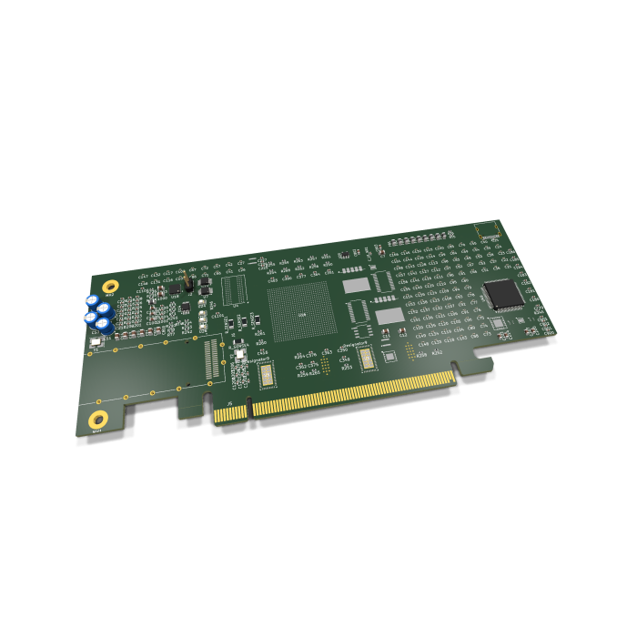
AutoPhi V19 PCIe 5.0 QSFP28 Optical - BGA-900 Editable KiCad Design Source
Editable KiCad design source for this AutoPhi board — fork it, modify it, tape it out at your foundry. Skip the schematic capture.
Why this is worth what it costs
Reusing a proven library means your engineering hours go into differentiation, not re-solving problems CRI-ONE already solved. What you are paying for is 15+ years of AutoPhi R&D, publicly documented since 2010 and patent-filed since 2012 — packaged as a frozen v1 you can drop into your design flow.
What ships in the license
All files needed to bring this asset into your design flow — source, layouts, netlists where applicable, and the corresponding foundry / EDA documentation. Delivered as an AES-256 encrypted downloadable archive.
What you own after the sale
The right to use, modify, and integrate this asset into your own products.
Derivative rights to spin variants without coming back to CRI-ONE.
Exclusive license for this implementation. No one else can ship this specific asset while you hold the license.
Priority-date defense
The foundational AutoPhi architecture is publicly documented from 2010 (Internet Archive) and patent-filed from 2012 (USPTO), under CRI-ONE’s name and independently verifiable. No prior art can invalidate the claims that come with your license.
© CRI-ONE. All rights reserved. Patents issued and pending. Unauthorized reproduction of the underlying designs is prohibited.
Extended catalog & full narrative — AutoPhi V19 PCIe 5.0 QSFP28 Optical - BGA-900 Editable KiCad Design Source
The extended dossier appended from the 2026-08-05 catalog snapshot. Prices in the body copy have been stripped; the live-store price on this page is the authoritative figure. Images have been omitted.
AutoPhi V19 PCIe 5.0 QSFP28 Optical — BGA-900 Editable KiCad Design Source
The complete, editable engineering design. Not gerbers. Not a datasheet. The actual KiCad project, opened and modified on your own bench.
What this is
This is the mid-range carrier — enough I/O for 16 to 32 SerDes lanes alongside a full DDR3 bank, without the routing density of the flagship. You receive the design as source: the full
hierarchical schematic, the routed board, every library the project
references, the 3D models, the ball-map spreadsheets, and a netlist
exported from the schematic so you can audit connectivity before you ever
launch KiCad. Open board/*.kicad_pro in KiCad 10 and the entire
project loads with its libraries already wired up.
AutoPhi ships blueprints. You take the design to whichever fabricator and whichever volumes you already trust — there is no tooling lock, no per-unit royalty, and no obligation to come back to us to build it.
The board at a glance
| Outline | 172.48 × 69.78 mm |
| Copper layers | 12 |
| Routed track segments | 6,707 |
| Vias | 969 — 969 through |
| Nets | 1,452 |
| Placed components | 523 across 3,136 pads |
| Schematic sheets | 20 |
Component census: 383 × C · 62 × R · 32 × U · 9 × FB · 8 × RT · 6 × TP · 5 × J · 4 × CS · 4 × CE
Layer stackup
Twelve copper layers in an HDI arrangement, with dedicated ground and power planes interleaved between the signal layers so every high-speed pair has a reference plane adjacent to it.
| 1 | F.Cu | signal |
| 2 | GND1 | signal |
| 3 | POWER1 | signal |
| 4 | POWER2 | signal |
| 5 | GND2 | signal |
| 6 | In5.Cu | signal |
| 7 | In6.Cu | signal |
| 8 | In7.Cu | signal |
| 9 | In8.Cu | signal |
| 10 | In9.Cu | signal |
| 11 | In10.Cu | signal |
| 12 | B.Cu | signal |
Copper pours: GND on 12 layers ·
Routing, layer by layer
| B.Cu | 1,225 segments |
| F.Cu | 1,873 segments |
| GND1 | 406 segments |
| GND2 | 261 segments |
| In10.Cu | 330 segments |
| In5.Cu | 417 segments |
| In6.Cu | 416 segments |
| In7.Cu | 394 segments |
| In8.Cu | 346 segments |
| In9.Cu | 392 segments |
| POWER1 | 266 segments |
| POWER2 | 381 segments |
Via geometry in use (pad / drill): 0.30/0.15 mm ×572 · 0.35/0.20 mm ×274 · 0.50/0.30 mm ×117 · 0.60/0.35 mm ×6.
Design rules and netclasses
This is an HDI-class design. Confirm your fabricator can hold these before quoting — the annular ring and laser drill sizes are the numbers that decide whether a shop can build it.
| Minimum track width | 0.0762 mm |
| Minimum clearance | 0.0762 mm |
| Minimum via diameter | 0.2032 mm |
| Minimum via annular ring | 0.05 mm |
| Minimum through-hole | 0.127 mm |
| Minimum microvia drill | 0.0762 mm |
| Hole-to-hole | 0.2032 mm |
Eleven netclasses are defined, so the router and DRC treat a PCIe lane differently from a 12 V rail rather than applying one global rule:
| Class | Clearance | Track | Via ⌀/drill | µVia ⌀/drill |
| Default | 0.15 | 0.15 | 0.35 / 0.2 | 0.2 / 0.1 |
| Control | 0.15 | 0.2 | 0.35 / 0.2 | 0.2 / 0.1 |
| DDR_ADDR | 0.1 | 0.125 | 0.35 / 0.2 | 0.2 / 0.1 |
| DDR_CLK | 0.1 | 0.125 | 0.35 / 0.2 | 0.2 / 0.1 |
| DDR_DQ | 0.1 | 0.125 | 0.35 / 0.2 | 0.2 / 0.1 |
| Ground | 0.15 | 0.4 | 0.5 / 0.3 | 0.2 / 0.1 |
| I2C | 0.15 | 0.2 | 0.35 / 0.2 | 0.2 / 0.1 |
| PCIe5 | 0.1 | 0.1 | 0.3 / 0.15 | 0.15 / 0.075 |
| Power | 0.15 | 0.4 | 0.5 / 0.3 | 0.2 / 0.1 |
| Power_12V | 0.3 | 0.6 | 0.6 / 0.35 | 0.2 / 0.1 |
| QSFP | 0.1 | 0.1 | 0.3 / 0.15 | 0.15 / 0.075 |
All dimensions in millimetres.
The schematic — 20 sheets
A hierarchical design, not one enormous page. The root sheet indexes the pages below; each is self-contained and connected by global labels, so the same net name means the same net everywhere in the project.
- 01 central processor — the BGA site itself — the accelerator's ball field, its decoupling and its escape fan-out
- 02 pcie retimers redrivers — DS80PCI810 retimers conditioning the PCIe lanes between the edge fingers and the die
- 03 pcie x16 edge connector — the x16 gold-finger interface, all 164 pins, with PCIe-spec pin naming
- 05 compute — the compute cluster and its local support
- 06 telemetry clock — clock generation and the telemetry path
- 07 optical thermal — optical front end and thermal sensing
- 08 esd protection array — ESD clamps on every externally exposed line
- 09 bracket i o connectors — the QSFP28 cages and bracket-edge I/O
- 10 mounting test — mounting holes, fiducials and test points
- 11 passives — the bulk passive population
- 12 retimer decoupling — per-retimer decoupling networks
- 13 pcie ac coupling — AC-coupling capacitors on the high-speed pairs
- 18 boot eeprom leds — boot EEPROM and status indication
- 20 clock si5351 — Si5351 programmable clock generation
- 21 charger usbc — USB-C side-channel and charging
- 22 esd protection — further ESD protection
- 23 telemetry — telemetry acquisition
- 24 mcu msp430 — the MSP430 housekeeping controller
- 26 heatsink mounting — heatsink mounting provisions
- 27 qsfp cage — the first QSFP28 cage
Everything in the download (5.9 MB)
- schematic/ — the root sheet plus all 20 child pages
- board/ — the routed
.kicad_pcb, the.kicad_proproject carrying the rules and netclasses above, and both library tables - libraries/ — every symbol and footprint library the design references, including the AutoPhi BGA symbols, the BGA-900 footprint, the 164-pin PCIe x16 edge connector, the DDR3 x16 FBGA and the DS80PCI810 retimer
- 3d/ — the 3D models used by the footprints, so the board renders and mechanically checks straight out of the box
- pinmaps/ — the ball-to-signal assignment as CSV, which is the document you will actually work from when adapting the design
- netlist/ — a netlist exported from this schematic (1,452 nets), so connectivity can be verified with a text editor and no KiCad install
- KNOWN-ISSUES.txt — see below
- README.txt — orientation and verification steps
Read this before you buy — known gaps
The signal path is complete and routed. PCIe 5.0, QSFP28 optical and DDR are laid out across 6,707 track segments and 969 vias, and pass DRC against the netclasses listed above. That work — the escape from the ball field, the lane routing, the plane structure — is where the value of this design sits, and it is finished.
The power regulation section is not finished. Five LDO regulators are placed but unwired, and marked do-not-populate. They also have no supporting passives: no input or output capacitors, no feedback divider for the adjustable regulator, no output-programming straps for the ANY-OUT part. Fitting them as drawn would give unstable regulators with undefined output voltages. Completing this section is circuit design work, not a wiring correction.
U1 is wired above its absolute maximum. It is a TPS75725 sitting on a 12 V rail against a 6 V limit, and will fail on first power-up as drawn. The intended architecture is a two-stage rail — 12 V into the 36 V-capable TPS7A4700, then 5 V into the low-voltage regulators — but that intermediate stage is part of the unfinished section above.
15 parts are marked do-not-populate and are excluded from the bill of materials and from both pick-and-place files, so an assembly house will not attempt to fit them:
J4— WonderPhi_TFU12— TSSOP-28U22— TPS75725U23— TPS735U24— SFH2400U26— SFH2400U27— SFH2400U28— SFH2400U30— SOT-23-6U42— TPS7A4700U43— TPS735U45— SOT-23-6U46— LP3878-ADJU47— SOIC-8 narrowU50— TSSOP-28
Five of those carry a package name where a part number should be — the component has not been selected yet, so nobody could wire them until it is.
Extension signals — yours to route
195 of 391 net-level connections are drawn. The remaining 196 show up in KiCad as ratsnest lines. That looks like an unfinished board on first opening, but the pattern here is deliberate.
The core interfaces are wired: PCIe 5.0 fingers to the die, QSFP28 lanes to the cage, DDR3 to the memory chip, the MSP430 management path, power and ground planes to every part. Those are the parts a fabricator needs to build a working card and are complete.
What the ratsnest lines mark is the extension surface. This is a reference design, and like any reference design or development board it exposes signals the die can provide but this specific variant does not spend. Additional QSFP lanes beyond the four used by the on-board cage. GPIO from the MSP430 left as convenient tie-off points. High-speed I/O pairs from the central processor that a downstream product would break out to a daughter card, a mezzanine connector or a second cage.
Route them if the derivative you are building uses them; leave them if it does not. KiCad 10's interactive router closes each connection in seconds with live DRC feedback. This is common on carrier-class designs and not a manufacturability issue: a bare pad with no track is fabricated as a bare pad with no track, and either way the underlying design intent stays intact.
Who this is for
Teams standing up a PCIe 5.0 accelerator prototype who would rather start from a routed HDI carrier than draw a 900-ball escape from scratch. The ball-field escape, the plane structure and the high-speed lane routing represent the largest block of layout time in a design like this, and it is done. What remains is the power section, which is well-defined work with a known architecture.
If you need a finished, fully-populated design you can send straight to assembly, this is not that, and the section above says so plainly. If you want the hard layout done and are equipped to close out a power tree, this will save you weeks.
Delivered as a ZIP (5.9 MB, 76 files). Licensed for your own fabrication and modification. Christopher Gabriel Brown — CRI-ONE.COM
b2eaea097a0dd5bfd2436c8a83e51080b2667097d6ee64d4abdc81719846e627
AutoPhi V19 PCIe 5.0 QSFP28 Optical - BGA-900 Editable KiCad Design Source
Publicly online since 2010 · U.S. patent applications since 2012 · inventions offered since 2014. The work of Christopher Gabriel Brown, independently documented.