
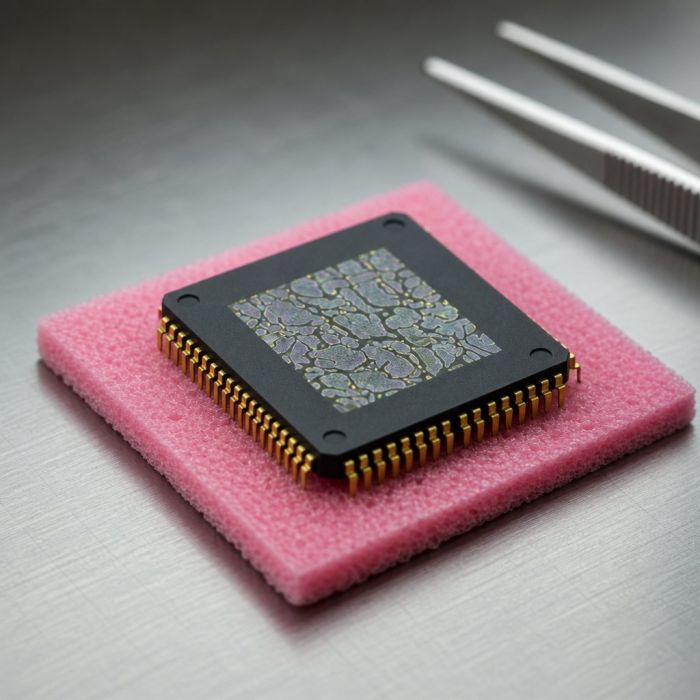
84-phantasmphi-cpu
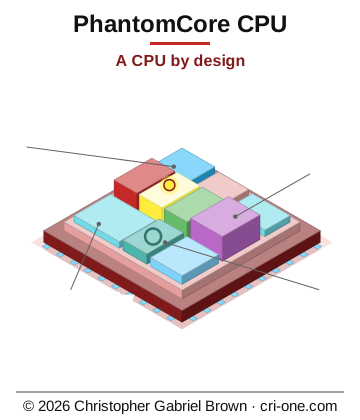
Asset valuation: $18,000,000,000. Project 84 · cri-one.com portfolio · Author: Christopher Gabriel Brown · 2026-08-21 A CPU by design. Project 83's QuettaPhantom proudly listed the three things it deliberately lacked — fetch, memory hierarchy, interrupts.
Think of the old pairing of a 386 and the math chip that sat beside it, one running the program and the other answering the hard arithmetic. PhantomCore makes that pairing literal on CRI-ONE's own seeds. Project 83's QuettaPhantom coprocessor openly listed the three things it left out: fetch, a memory hierarchy, and interrupts. Project 84 builds exactly those three, on purpose, on the same lineage. The CPU runs the program, the phantasm engine answers the math as a memory-mapped coprocessor, and a completion interrupt joins the two.
Two proven generations ship together. PHC01 set the architecture: fetch, decode and execute over an original 32-bit instruction set with sixteen registers (not a RISC-V, ARM or x86 copy), a three-tier memory hierarchy, vectored interrupts, and a color math ALU where add is red, multiply is yellow and divide is green. PHC02 keeps every instruction-set promise identical and brings three engineering improvements: SRAM macro scratchpads in place of flip-flop arrays, a sequential divider that takes the divide off the critical path, and a two-cycle deterministic fetch. Both generations run the same hand-assembled fifty-one-instruction program that exercises every claimed feature and judges its own correctness, and both report ALL CHECKS PASS.
This is a blueprint for engineering buyers and licensees who want a CPU that is RTL-proven, SKY130-mapped and ready for foundry handoff. The buyer walks away with a completed design whose self-test has been proven end to end on both generations; the inventions underneath stay with the inventor.
Description
The full processor built on AutoPhi seed lineage. Light-Trigger-lineage ISA. Phantasm math coprocessor. QBeam ExitPhi fabric. 1,200 nano layers. Ten technologies × four axes at Quetta.
PhantomCore CPU (SKU 2115)
Inventor: Christopher Gabriel Brown — Inventor · Author · Visionary.
Patent reference: USPTO Application No. 19/722,805 (QBeam ExitPhi integrated interconnect fabric); USPTO Patent 18/370,908 (LED nano-array photon pump).
Project: 84 — PhantasmPhi CPU line — cri-one.com portfolio.
Status: RTL-proven (L2) + SKY130-mapped. PHC01 self-test PASSES. PHC02 self-test PASSES. Design complete. Foundry handoff ready.
Maturity date: PHC01 first PASS 2026-08-21; PHC02 first PASS 2026-08-22.
PhantomCore is the full CPU built on the AutoPhi seed lineage. Project 83’s QuettaPhantom coprocessor proudly listed the three things it deliberately lacked — fetch, memory hierarchy, interrupts. Project 84 builds exactly those three, on purpose, on the same seeds. The CPU runs the program; the phantasm answers the math; the interrupt joins them — the FPU beside the 386, made literal.
Two proven generations ship together. PHC01 established the architecture: fetch/decode/execute over the original Light-Trigger-lineage ISA, a three-tier memory hierarchy, vectored interrupts, the color_math_alu seed as every arithmetic path, and the phantasm_math_engine as a memory-mapped coprocessor with completion interrupt. PHC02 keeps every ISA promise identical and delivers three concrete engineering improvements: SRAM macro scratchpads, a sequential divider dispatch, and a two-cycle deterministic fetch.
Instruction Set Architecture — Light-Trigger-Lineage ISA
Original 32-bit ISA. Not a RISC-V, ARM, or x86 copy — per the seed’s own founding claim. 16 general-purpose registers (r0 hardwired to zero). Encoding: [31:28] op | [27:24] rd | [23:20] ra | [19:16] rb | [15:0] imm .
32-bit RISC · 16 registers · Light-Trigger-lineage ISA (original, not RISC-V/ARM/x86).
Color Math ALU — ADD = Red, MUL = Yellow, DIV = Green. Every instruction computes in the same wavelengths as every AutoPhi core and every phantom. DATA_WIDTH = 64. Precision mode = 2’b11.
Phantasm coprocessor — phantasm_math_engine (PACK_ID 0x04) as MMIO device with completion interrupt.
Vectored interrupts — vector = word address 2. Three sources: timer, phantasm-done, external pin. EPC/CAUSE/IE registers. EI/DI/IRET instructions.
Memory hierarchy — register file (L0) → L1 I/D scratchpads (1-cycle) → MMIO device tier (multi-cycle).
Multicycle FSM — ~2–4 cycles/instruction at the seed ALU’s pace.
PHC01 — First-Generation Silicon
Self-test result PHANTOMCORE: ALL CHECKS PASS.
Maturity note Scratchpads synthesize as flip-flops and dominate 55% of die area; PHC02 resolves this
PHC02 — Second-Generation Engineering
PHC02 keeps every ISA promise identical to PHC01. Three concrete changes from the PHC01 roadmap:
PHC02 · SRAM + sequential divider + two-cycle fetch · proven
1. SRAM macro scratchpads — sram_1rw wrapper (49 lines) replaces flip-flop arrays. Sync-read, sync-write, single-port. Maps 1:1 to sky130_sram_1rw macro at OpenLane P&R substitution. Behavioral in simulation ( SIM_INIT guard), black-box in hardening. Write-first semantics matching sky130 macro default.
2. Sequential divider dispatch — seq_divider.v (77 lines). 32-cycle restoring divider, non-pipelined. Removes DIV from the seed ALU’s combinational critical path. Divide-by-zero saturates to all-ones, matching the seed. PHC01 forced CLOCK_PERIOD 500 ns because of the combinational 64-bit divide; PHC02 removes that anchor.
3. Two-cycle deterministic fetch — S_FETCH_ADDR drives imem_addr combinationally from pc ; S_FETCH_WAIT latches SRAM output into ir . Straight-line cost: 2 cycles/instruction.
Yosys standalone cells 44 cells, 459.19 µm² (note: standalone Yosys constant-folds SRAM — apples-to-apples number requires OpenLane P&R with sky130 SRAM macro library)
Both generations run identical hand-assembled machine code ( phantom_program.hex , 51 instructions) that exercises every claimed feature and judges its own correctness in software :
Step Test Proof
1 MUL 6 × 7 on the color ALU Store result (42) to L1 data scratchpad at address 0x100, load back through the hierarchy, verify equality via BNE → fail
2 EI + arm one-shot timer (50 ticks) Spin until vectored timer interrupt taken at word address 2. ISR reads CAUSE (0x3FC), acknowledges via IRQ_ACK (0x3F1), increments r10 tick count, IRETs. Software verifies r10 > 0
3 Wake phantasm coprocessor via MMIO Deposition D05 KELLY (p=0.75, b=1.0). Completion interrupt taken. Software reads PH_RES_LO (0x3F9), expects 32768 (0.5 in Q16.16 fixed-point — the proof-battery value), verifies via BNE → fail
4 Debug protocol Write #1 = timer ticks seen (must be > 0). Write #2 = 0x00000001 PASS (or 0x00000BAD FAIL). HALT.
0x000–0x2FF L1 data scratchpad (768 words PHC01; 1,024 words PHC02) Read/write, 1-cycle (PHC01), sync SRAM (PHC02)
Every arithmetic instruction executes on color_math_alu (shared from Project 83, not copied). The CPU computes in the same wavelengths as every AutoPhi core and every phantom.
Project 83’s phantasm_math_engine sits beside the CPU as a memory-mapped coprocessor with a completion interrupt. PACK_ID = 0x04.
400 GB/s bidirectional — 25.6 GT/s per lane × 16 lanes.
400 ns cut-through latency — wire-speed probability transfer.
PCIe 5.0 x16 HHHL — standard slot, standard power.
CoolBeam thermal management — optical idle links, zero standby power on unused lanes.
PipeBeam ordering — in-order delivery, zero reordering overhead.
12 silicon configurations — 22 nm → 2 nm node coverage.
No cables. No third-party silicon. No licensing fees.
QBeam ExitPhi is the interconnect fabric that binds PhantomCore CPUs to phantasm coprocessors, to fleet neighbours, and to host systems. Every PhantomCore die carries the ExitPhi PHY on-die — the CPU, the coprocessor, and the interconnect are one piece of silicon.
GOPS · Ronna · Quetta — Full Performance Ladder
Quetta Summit 10³&sup0; Full architecture: 1,200 layers, 480K voxels, 12.7M facilities, all axes maxed
100 rungs at ×1.61758 per rung. From measured 2.1 GOPS silicon foot to 10³&sup0; Quetta. Each rung is a concrete architectural checkpoint. The ladder is the product.
V20 Epiphany architecture. AES substrate (400 W/m-K). Each step a modest multiple of the last:
OUT · 480K voxels UP · 1,200 layers ACROSS · 12.7M facilities SMALLER · ~1.5 nm
2 LED Nano-Array (8×10¹&sup0;/cm², Patent 18/370,908) Photon pump for quantum battery charging
3 Photon Energy Storage (E=hf) Self-power: photon emission → re-absorption → coherence storage
Real quantum. Not simulated gate-logic. Not classical approximation.
- Silicon quantum dots (3–10 nm) — discrete energy levels, Zeeman/Landau splitting
- Photon-driven energy storage — E=hf, 250–300 nm UV photons, LED nano-array (8×10¹&sup0; LEDs/cm², Patent 18/370,908)
- Quantum superposition charging — multi-state occupation, coherence time > gate time
- 84–98% photon recycling — emit → absorb → re-emit loop gated by QEC surface code
- Self-power doctrine — quantum battery layers generate and store their own operational energy
Liberty file: sky130_fd_sc_hd__tt_025C_1v80.lib (official SkyWater 130 nm, typical-typical, 25°C, 1.80 V).
Yosys version: 0.58+138 (git sha1 3d5b1e0a9).
Synthesis tool: ABC logic synthesis + Yosys dfflibmap .
rtl/phantom_core_cpu.v 212 PHC01 CPU core — fetch/decode/execute FSM, color ALU integration
rtl/phantom_soc.v 150 PHC01 SoC — memory hierarchy, timer, IRQ controller, phantasm coprocessor
rtl/tb/phantom_soc_tb.v 59 PHC01 self-test bench — runs to HALT, judges debug protocol
rtl/sw/phantom_program.hex 56 Hand-assembled Light-Trigger ISA machine code (51 instructions)
rtl/phc02/phantom_core_cpu_v2.v 234 PHC02 CPU core — SRAM fetch, sequential divider dispatch
deploy_phantomcore_cpu.php Magento deployment script (SKU: CRIONE-PHANTOMCORE-CPU, category 3428)
Generational Law
Each PHC generation must list lower per unit of capability than the prior generation. PHC02 satisfies on two axes:
- Cycles per instruction on straight-line code: PHC02 = 2 c/i (same as PHC01), but the removed combinational DIV means the clock can uplift when real P&R replaces the 500 ns period. Effective ops/s rises.
- Die area per unit of function: PHC02 replaces ~55% of PHC01 area (scratchpad FFs) with SRAM macro area, which at SKY130 shuttle shrinks substantially per bit.
Proven: RTL simulation self-tests pass end-to-end (PHC01 + PHC02). SKY130 synthesis mapping complete (PHC01).
Not yet: SDC timing constraints, OpenLane place-and-route (queued behind the QEMU forge), tape-out, silicon.
No pipelining — F/D/X/M/WB stages remain multicycle (PHC02.1 target).
No caches — scratchpad is still the L1 (PHC03 roadmap).
No PHC02 P&R yet — OpenLane run queued; Yosys standalone area check is not fair (constant propagation folds the SRAM design).
Firewall: Project 83 supplies the seed ALU and the phantasm coprocessor at arm’s length; no revenue or contracts co-mingle.
Pricing rule 2× the QuettaPhantom coprocessor ($212,500,000,000) — a CPU commands double its coprocessor
Restrictions No PRC/RU entities. US export law. US companies only. USD only.
Deliverable RTL source (Verilog). Never free, never naked.
PHC02 RTL phantom_core_cpu_v2.v , phantom_soc_v2.v , sram_1rw.v , seq_divider.v , phantom_soc_v2_tb.v
Build artefacts Compiled simulations (.vvp), SKY130 gate-level netlists, synthesis logs
This package ships on a single Blu-ray disc, posted to the delivery address on your order. The archive on the disc is AES-256 encrypted; the passphrase is sent separately, by email, once the disc is despatched — so the disc alone is of no use to anyone who intercepts it.
Discs are despatched by tracked, signed-for post. Allow 5 business days for mastering and verification before despatch.
Email and postal mail only. No phone calls, no brokers, no intermediaries.
Available exclusively to companies incorporated, headquartered, and primarily operating in the United States of America. USD only.
© 2026 Christopher Gabriel Brown. All rights reserved. CRI-ONE · cri-one.com portfolio · Project 84. Not offered to PRC/RU entities.
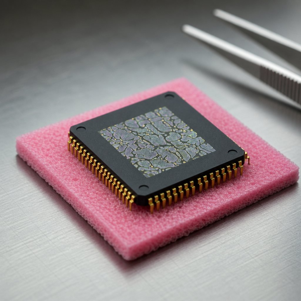
Photo
Footnotes
- Product number 8534.
- Family: phantasmphi.
- Purchase: When you buy, you buy the use of that blueprint only.