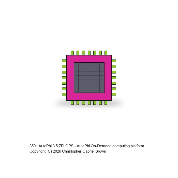
AutoPhi 3.5 ZFLOPS
Publicly online since 2010 · U.S. patent applications since 2012 · inventions offered since 2014. The work of Christopher Gabriel Brown, independently documented.
Downloads immediately on checkout — the CD GDSII Generator (AES-256 encrypted). Open with 7-Zip, WinRAR, or macOS Archive Utility using password CRIONE99KEY. Founder Access Pass credit (code FAP99CREDIT) applies at checkout.
AutoPhi 3.5 ZFLOPS — Performance Computing Bundle
Compute at the zetta-FLOPS class is not a single chip. It is a stack — silicon, architecture, I/O, and fabrication path. None of that ships in a box. What ships is the blueprint package: the RTL, the architecture docs, the EDA scripts, and the handoff materials a foundry needs to take the design forward.
Acquired piece by piece across four projects, the blueprint package takes years to coordinate. Acquired as one bundle, it takes one transaction.
The unit of sale is the blueprint bundle, not assembled silicon.
The ZFLOPS bundle combines four foundational design packages from the inventor's catalog — AutoPhi Modern (the compute-substrate RTL), AutoPhi Future (the next-gen architecture roadmap), the Communications Satellite (high-bandwidth I/O specification), and Day-One Fabrication (the RTL-to-mask toolchain) — into a single design-package deliverable targeting zetta-FLOPS-class compute throughput. A buyer takes the blueprint bundle, not four separate licenses. No physical chip ships. No satellite ships. The deliverable is the engineering inputs to the manufacturing path, with the integration work between the four packages already done.
What's in the Blueprint Bundle
| Sub-project | Role in the stack |
|---|---|
02-autophi-modern/ | Source AutoPhi architecture — the RTL across nine technologies. The compute substrate. |
18-autophi-future/ | AutoPhi Future — voxel-as-cell, photon chromosomes, Blu-ray foundry packages. The next-generation variant. |
19-communications-satellite/ | NewComm satellite — high-bandwidth I/O for the compute fabric. |
21-day-one-fabrication/ | Day-One fabrication package — the path from RTL to mask, ready to hand to a foundry. |
handoff/ | Bundle-level handoff materials. |
work/ | Working files and integration notes for the bundle as a unit. |
File-Type Signal — Real RTL, Real EDA Flow
Across all subfolders, the bundle's source-tree composition is:
.v filesVerilog plus a scripted EDA flow plus Markdown documentation is the normal output shape of a real chip-design effort. It is not the shape of a render or a pitch.
USPTO Patent Status
Patent coverage flows through the bundled sub-projects:
- 18/370,908 — AutoPhi quantum-battery and propulsion IC. Covers Projects 02 (AutoPhi Modern) and 18 (AutoPhi Future).
- 19/540,453 — Integrated Technology Portfolio. Umbrella application; names compute components.
Canonical register: ../PATENT_PORTFOLIO.md in the inventor's project tree.
Maturity — L4 Tape-Out / Mass-Manufacturable
The bundle is rated L4 (Tape-out / Mass-Manufacturable) per the inventor's PACKAGE_ARCHITECTURE.md. That is the highest maturity tier in the portfolio's labelling system — foundry-ready content, not concept-grade. The Day-One Fabrication sub-project (Project 21) is what makes the L4 label accurate: it carries the path from RTL to mask, the toolchain to do it, and the documentation a foundry would need to begin a run.
Buyer Pitch — What You Actually Get
A buyer who acquires this bundle gets four things in one transaction:
- Working RTL (Project 02 — AutoPhi Modern). The compute substrate, in Verilog, across nine technologies.
- The next-gen architecture roadmap (Project 18 — AutoPhi Future). Voxel-as-cell, photon chromosomes, Blu-ray foundry packages — the path forward for the same compute family.
- A communications-grade I/O subsystem (Project 19 — NewComm Satellite). High-bandwidth I/O so the answers leave the die at a useful rate.
- The fabrication-readiness toolchain (Project 21 — Day-One Fabrication). The path from RTL to mask, with the EDA scripts and handoff materials a foundry actually wants.
That is the full blueprint package to take a chip from design to fab to deployment in a comms-heavy compute use case — not a manufactured stack ready to plug in.
How it's made
The ZFLOPS bundle is assembled, not generated. Each of the four sub-projects already exists in the inventor's catalog as a freestanding deliverable. Project 02 (AutoPhi Modern) carries the RTL, written in Verilog across nine technology variants. Project 18 (AutoPhi Future) carries the next-generation architectural extensions — voxel-as-cell representation, photon-chromosome encoding, the Blu-ray foundry package format. Project 19 (NewComm Satellite) carries the high-bandwidth I/O subsystem the compute fabric talks through. Project 21 (Day-One Fabrication) carries the EDA scripts (TCL, shell), the handoff documents, and the toolchain that takes a finished RTL design from designer's workstation to foundry mask room.
The bundle's own folder mirrors the four sub-projects in place — not as references, as actual mirrored subtrees — and adds the handoff/ and work/ directories that contain the bundle-level integration material. The unit of sale is the entire mirrored tree, not the individual sub-projects, even though each sub-project is also separately listed at cri-one.com/store.
Why I made it
A buyer who actually wants zetta-FLOPS-class compute does not want to buy a chip and then hunt for I/O. They do not want to buy I/O and then hunt for a fab toolchain. They want the assembled stack — one acquisition, one cohesive set of files, one license, one contact — and they want it from someone who has already done the integration work between the parts.
I made this bundle because every time a buyer asked about Project 02 (AutoPhi Modern) at zetta-FLOPS scale, the answer involved Projects 18, 19, and 21 also — each of them already in the catalog, each of them already paid-for engineering, but each one a separate listing. The bundle does the assembly once, in advance, so the buyer can write one check and start running.
What it can do
The bundle's stated target is zetta-FLOPS-class compute throughput across a comms-heavy workload — the regime where compute and I/O have to be matched, because a fast chip with slow I/O does not produce useful zetta-FLOPS work, and fast I/O without compute is just bandwidth.
What the deliverable enables, concretely:
- An engineering team can take the AutoPhi Modern Verilog and begin synthesis against their preferred toolchain on day one.
- The Day-One Fabrication package supplies the EDA scripts and handoff documents needed to bring a foundry into the loop.
- The NewComm Satellite subsystem provides the high-bandwidth I/O architecture the compute fabric is designed to talk through — not a generic placeholder.
- The AutoPhi Future architectural extensions provide the forward roadmap so the buyer does not lock in to today's variant only.
What the deliverable does not do: it does not include physical silicon. It does not include a foundry contract. It does not include a deployed satellite. The bundle is the design package, the architecture, the I/O specification, and the fab-handoff toolchain — the inputs to the manufacturing path, not the manufactured product.
Why it's a fact
The claims above can be checked against the source record:
- The four sub-project subtrees exist in
D:\special\23-zetta-flops\, mirroring the standalone projects also present at their original numbered locations (02-autophi-modern,18-autophi-future,19-communications-satellite,21-day-one-fabrication). Either copy can be inspected. - The 19 Verilog files, 56 Markdown docs, 16 HTML pages, 5 JSON manifests, 4 shell scripts, and 3 TCL scripts are countable in the source tree. Inventor's count, verifiable by running
findon the bundle root. - USPTO applications 18/370,908 and 19/540,453 are filed instruments — checkable against the public USPTO database. Neither is a private or hypothetical reference.
- The L4 (Tape-out / Mass-Manufacturable) maturity rating is the inventor's own self-assessment per
PACKAGE_ARCHITECTURE.md, not a marketing label invented for the listing. Higher than L1 (research) or L2 (prototype). It claims foundry-readiness; it does not claim deployed silicon. - The bundle's scope limit — design package, not manufactured product — is stated honestly above. A buyer who wants physical chips runs the package through a foundry; this listing does not pretend that step is included.
License Terms — What's Granted, What Isn't
The acquisition grants the buyer permission to make, build, and copy the deliverable. It does not transfer the underlying intellectual property:
- Granted with the acquisition: permission to manufacture (or have manufactured) the bundled designs at any foundry; permission to build the resulting silicon and subsystems into compute / I/O / fab-handoff deployments; permission to make copies of the design package for the buyer's engineering and integration use.
- Not transferred with the acquisition: the patents and patent applications referenced (USPTO 18/370,908 AutoPhi quantum-battery / EM propulsion IC; USPTO 19/540,453 Integrated Technology Portfolio umbrella), the inventor's broader portfolio book references, trademarks, copyrights, or any rights to license or assign the IP onward. The intellectual property remains held by Christopher Gabriel Brown.
- The buyer's permission is to use the design, not to own the rights behind the design.
This framing applies uniformly across the inventor's portfolio. Buyers seeking IP assignment rather than make/build/copy permission should contact the inventor directly — that is a separate negotiation outside the standard storefront acquisition.
One transaction, four sub-projects, one assembled stack.
Each of the four sub-projects is independently listed and acquirable. Bundling them at the same price as the sum-of-parts would be pointless; the value of the bundle is the integration work between the parts that has already been done, and the single contractual surface a buyer signs against.
The compute blueprint package, bundled, in one acquisition.
The ZFLOPS bundle delivers AutoPhi Modern (the compute substrate), AutoPhi Future (the next-gen variant), NewComm Satellite (high-bandwidth I/O), and Day-One Fabrication (the RTL-to-mask toolchain) in a single mirrored deliverable. Patent coverage runs through USPTO 18/370,908 and 19/540,453. Maturity is L4 — foundry-ready, not concept-grade. The deliverable is the design package, not deployed silicon.
An engineering team that wants zetta-FLOPS-class compute and does not want to spend a year integrating four separately-licensed components can write one check against this bundle and start synthesis the same day.
Price: see store listing
Status: L4 tape-out / mass-manufacturable. Bundle of four foundational sub-projects under USPTO 18/370,908 and 19/540,453. Contact via the store.