
AutoPhi Monolith Variations
A complete computer on one die, in two PCIe form factors. The AutoPhi Monolith slab — compute, CRAM memory with shape, quantum battery, programmable secure mirror, per-layer EM cooling — shipped as the full design license plus one DPU card (Nexus profile) plus one Accelerator card (REV, Train, Infer, Vision, Lingua, Spike, Qubit, Scale, Edge). Design package; GDSII generator ships; stream does not. Patent pending through its parts, all equally.
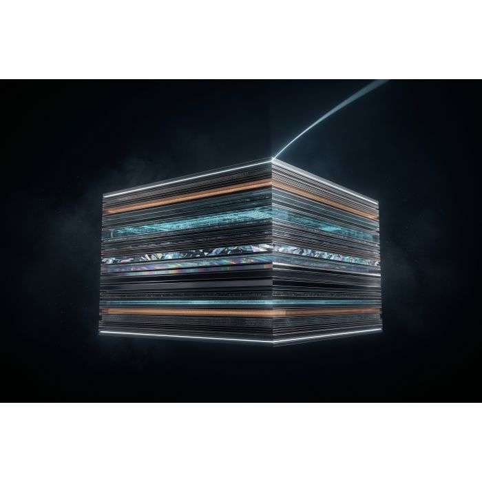
Picture a brick of silicon a hand would cover, suspended in a dark room. It is not plugged into anything — no cables, no sockets, no fan, no heatsink, no battery pack beside it. From one top corner, a single thread of coherent light rises and disappears into the dark. That thread is the only thing leaving the slab. Everything else is inside it: the compute, the memory, the storage, the battery, the cooling, the security, the timing, the law, and the program that decides what the slab is pretending to be this hour. The inventor's words for the posture: same ISA, thicker silicon. A brick of silicon that is a complete computer, not a chip that needs a computer around it.
Look closer and the brick is a stack, not a block. Where every earlier AutoPhi generation stacks compute layers — the vertical threading that puts 120,000 through-silicon vias per square millimetre at APM05 and 500,000 at APM08, carrying 400 to 1,200 active compute layers through 3.5 to 7.0 millimetres of silicon — the Monolith stacks more than one kind of layer in the same slab. Some layers are the compute lattice itself. Some are CRAM cells whose shape is read as part of the data — a memory where what the cell looks like is part of the answer. Some are quantum battery layers, up to 192 of them per die, holding the slab's own stored charge; others are the at-will-recycle layers that join storage, generation and recycling in one battery so the slab performs on demand instead of waiting on an external power feed. Some layers are the programmable secure mirror, encrypting at silicon, with a chip-port storage identity that doesn't ask the operating system to hold a secret. Some layers are per-cell electromagnetic cooling, pushing 98.5 to 99.9 per cent efficiency across generations with no spinning parts. Some carry the light channels — nanophotonic links that move up to 28 petabytes per second between stacked layers at APM05.
Every kind of layer was named by the inventor in 2017, and dated. The Invent Depositions book (ISBN 978-1-979767897, published 2017-11-24) carries all 1,757 entries. The Monolith's roots are specifically: the solid-state data format thesis at entry #103 — "a 3.5 solid state data format would work; study of density of a disc/form is the goal"; the memory-with-shape at entry #86 — "CRAM data shapes; things to come and why data should have a shape; critical random access memory"; the encrypted-mirror chip at entries #722 and #723 — "open source programmable secure chips that are conveniently encrypted for resale as mirrored and embedded"; the at-will battery recycle at entry #1026 — "battery that incorporates the use of an at-will performance and storage with an added electrical generator and recycle"; the programmable-chip-as-appliance at entry #1060 — "programmable chip software and the opportunity to make a chip into a performance enhancer such as a co appliance or main appliance or second appliance for processing or for storage or routing"; and underneath all of them, the staircase mirror chips at entry #1, patent 3561 — the optical primitive that becomes the LED power recycling, the Reflective Tunnel, and the photonic I/O. The Monolith is the first slab in the portfolio where every one of those stacks together in the same silicon, not in separate products.
The slab's rhythm is kept by the Mainframe, the timekeeper from Project 121, brought down to die scale. Every one of the stacked cells sends a short telemetry frame to the Mainframe at a 1-millisecond tick, reporting where its beat landed in the last cycle. The Mainframe reads six match factors — rhythm, pitch, phase, timbre, dynamics and tempo — and sends the cell its next cycle time. The retime formula is on paper: T_c = T_ref × (1 − α × (SOC − SOC_REF)) × (1 + K_T × (T_chip − T_REF)), with a KP_PLL phase correction added only when the lock is held, the match sweet spot at R* ≈ 1.68, and the rhythm cliff at 0.693. When a cell loses the lock for four consecutive cycles the Mainframe holds the chip's own time while the cell's own tracker brings the peak back and the drive softens to the phase match. The firmware passes 41 of 41 checks in its default walkthrough on this machine. Nothing in the slab speeds up by playing faster; the inventor's rule is adding momentum means tightening the lock, not ignoring the chip and spinning.
Every write to the slab is law-checked by the Prodigal safety driver from Project 86. The law is the 10 Commandments and the Constitution, 11 byte-identical files that are never amended; a write that fails the gauntlet is refused in silicon, not in software. The safety driver's gauntlet currently passes 38 of 38 adversarial cases, including the two LED-counter rollover edges at the 48-bit wrap and the stuck-peak case that holds the cycle above the rhythm cliff. The fingerprint on GDS layer 254, from the Project 67 generator, is written into every GDSII the slab's buyer produces — the layout carries the licensee identity forensically from first etch, and no two buyers' streams carry the same stamp.
Role is chosen by the loaded program, not by the silicon. The Monolith inherits the ten per-generation accelerators from Project 02 AutoPhi Modern: Scale (CPU), REV (GPU), Nexus (DPU), Train and Infer (AI), Vision, Lingua (LLM), Spike (Neuromorphic — up to 80 million neurons and 2,400 PetaSynOPS at APM05-N), Qubit (Quantum — up to 10,240 logical qubits at APM05-Q, 350 million logical at the 15-smd AES-YFLOPS line) and Edge. The same slab can run as a CPU, as a GPU, as a storage controller, as a router, or as a hardware security module — whichever accelerator profile the owner loads into the programmable-chip-as-appliance layer. One quantum-classical hybrid ISA holds across every role, so the switch between them is a program load, not a re-architecture; APM12 adds three compute strands — electron, atomic and photon — that share the same ISA.
I/O is photonic only. The slab's one external contact is light: nanophotonic data flow inside the stack, QBeam between the slab and anything beyond it. Project 76 QBeam Transfer runs at a 1-millisecond tick with a 140-microsecond round trip and carries the Mainframe's registers to every cell at the inventor's 75-watt card figure for the full fabric. No copper leaves the slab for signal; no copper enters the slab for power, because power lives in the quantum battery layers (up to 192 per die) and recharges from the LED emission the stack produces as a byproduct of compute — 64 per cent net power reduction across 585 LED surfaces at APM05, 73 per cent across 1,200 surfaces at APM08, 90 per cent at PCIe REV-5, and 40 to 60 per cent when the same primitive runs at tower scale in Project 114.
What is new in this slab, and nowhere else in the portfolio yet, is the poly-stack. Project 28 AutoPhi Complete Unit integrates the nine Ultimate Technology interfaces on one die, but it still assumes external storage and external power. Project 85 AutoPhi V21 Ascension stacks all the way to 3,430 compute layers at APM12 Members tier, but the battery and the storage aren't inside the stack as data. Project 114 Super Magnum Quantum carries all nine at tower scale — 32 floors, 416 racks, 26,624 dies, 39.94 MWh of design reservoir — but it is a building, not a chip. The Monolith is the die-scale compression of the tower, and the first slab in the portfolio where nothing is plugged in except light.
On the inventor's five-level maturity ladder the Monolith is a design concept filed today — 2026-11-15 — at Level 0, with each of its parts pending at the level that part has reached in its own project: the Mainframe tempo tracker at L3 specified and simulated with firmware passing 41/41 of its default walkthrough; the AutoPhi Modern gen ladder published from APM01 through APM12; the Project 05 Quantum Battery LED power recycling circuit in RTL at led_power_recycling_circuit.v; the GDSII generator at Project 67 in shipping form. The slab's own gen number is left open; the natural slot is above APM12 because the Monolith adds layer kinds, not just layer counts. The silicon slab size — whether the Monolith inherits APM08's 7.0 millimetres or names its own — is open too. Both are the owner's call; nothing in this page commits to one.
What ships: the design package itself (README, SPEC, PATENT_POSITION, IP_REFERENCES, DESIGN_BRIEF); the GDSII generator as a working copy of Project 67 — the generator, never the stream, per the inventor's standing rule that generated GDSII files are too large and hinder production; the Prodigal safety driver's eleven law files; the Mainframe tempo tracker reference firmware; the AutoPhi Modern gen READMEs the Monolith inherits; and the IP ledger entries cited in the parts list. The buyer runs the generator on their own hardware; the fingerprint stamps their identity onto layer 254 of every GDSII they produce; their layout is theirs, and never exists on CRI-ONE systems. Delivery: Blu-ray, mailed. Settlement: direct, through the usual CRI-ONE channels on cri-one.com. The $1 billion figure is the full stack license as drawn here — the slab, the generator, the safety driver, the Mainframe firmware, the inherited gen READMEs, and the two PCIe cards (DPU + Accelerator) together — not a re-license of each part's own project.
The Monolith is patent pending through its parts, all equally. Non-exclusive. USA companies only. USD only. Email and postal mail only. The price is the owner's figure, set 2026-11-15.
Valuation
Product name: the Mainframe Summ. Project 121.
Pre-production blueprint usage right, patent pending through its parts, non-exclusive. The Mainframe Summ sits where three markets meet: compute hosting and AI infrastructure (one tower carries the reactor's whole rack floor: 100 tables, 10,000 cards, a design throughput of 20 exaOPS, extrapolated, not measured), battery energy storage and pulse power (26,624 quantum battery dies, 39.94 MWh design reservoir, 4.16 – 10.40 MW peak at the terminals), and district heating and cooling (its cold side sells cold off-season and its heat loop sells heat).
Patent position
Patent pending through its parts, all equally: the quantum battery chip (U.S. application 18/370,908), the CMOS sequencing umbrella (U.S. application 19/540,453), the all-in-one umbrella (U.S. application 19/835,210), and the reactor-scale compute facility and its continuation-in-part (U.S. applications 19/865,419 and 19/865,443).
Market opportunity
- AI-compute infrastructure: the category's recent precedent band runs from about $23B to $157B, median about $62B (as used for the QRS-118 listing).
- Battery energy storage systems: about $51B (2025) → $106B (2030) (as used for the Summ Engine listing).
- District energy: the Negative Microwave utility plant sells district cooling off-season; the heat loop sells heat.
Comparable transactions
- No public sale of a comparable pre-production package is on record.
Listed price
$1 trillion, set by the owner.
What moves the value up
- The bench sweep the principle paper asks for: one afternoon, the cycle swept from 5 ms to 2,000 ms on a quantum battery die, the charge per cycle recorded.
- A measured quantum battery die.
- One barrel built with its ring of cells and its tracker closed, the six match factors read off it.
- One Tower built and metered for a year with its tables running.
Maturity marker
L3 — specified and simulated; the figures that wait on first silicon at L1. At L3: the tower is specified from the Summ Engine's own sheet; the manager is written as firmware with a one-day simulation that runs and passes its checks, as a C port and as Verilog with a bit-accurate model; one parameter sheet with 113 checks feeds every file; the inherited Magnum controller and firmware stand at L3 on their own status. At L2: the tower and campus model (OpenSCAD). At L1, as design values unverified in silicon: the quantum battery die's 1,500 Wh and its 75 MW burst, the chip's settling time and Q, and the reactor card's throughput (extrapolated). L4 is the next step: a first article built and measured.
Description
AutoPhi Monolith Variations (SKU 122)
Patent status: Patent pending through its parts, all equally. Rooted in the inventor's Invent Depositions (CreateSpace, ISBN 9781979767897, 2017-11-24) and the modern AutoPhi continuation-in-part family (parent U.S. application 18/370,908 and its descendants).
A complete computer on one die. The portfolio already stacks compute layers in a growing count; the Monolith is the first slab where more than one kind of layer stacks. Compute, storage, power, cooling, security and role all live in the same silicon slab, pending through their parts.
What is new vs the closest things already in the archive: Project 28 AutoPhi Complete Unit integrates the nine Ultimate Technology interfaces on one die; it still assumes external storage and external power. Project 85 AutoPhi V21 Ascension (APM12) stacks more layers; battery and storage aren't inside the stack as data. Project 114 Super Magnum Quantum carries all nine at tower scale, 32 floors; the Monolith is the die-scale compression. The Monolith is the first slab where nothing is plugged in except light.
Same ISA, thicker silicon. The Monolith is not a new ISA. It is the AutoPhi Modern ISA stacked with more layer kinds. Which APM gen number the Monolith receives is the owner's call.
What does not ship: no generated GDSII (the files are too large and hinder production); no re-license of each part's project (the Monolith license is a stack license over the slab as drawn here); no tape-out, no shipping silicon.
Delivery. Design package on Blu-ray, mailed. Both PCIe cards shipped by insured carrier with signature on delivery.
Settlement. Direct, through the owner's usual channels on cri-one.com.
| Date Launched | 2026-11-15 00:00:00 |
|---|