
ICWritePhi — Full Family Blueprint
ICWritePhi
Stencil Graphic Laser Printer · Layer-Material Kits · Slicer & Router · 3-D Stack Process · Clamp Package · Paid Stencil Library
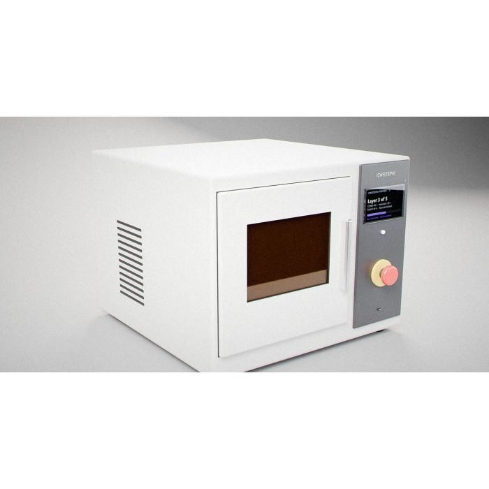
Desktop printed-chip fabrication. The sibling of WritePhi: same kitchen-table buyer, a different way to make the chip.
Six-SKU family flow. © 2026 Christopher Gabriel Brown · cri-one.com · ICWritePhi Project 110.
What it is
A six-SKU printed-chip fabrication product family for classrooms, R&D labs, small defense workshops and the maker community. A bench-top printer uses a commodity monochrome LCD as a dynamic stencil, images it through reduction optics so that a large pixel grid becomes a micron-scale connected circuit, cures or laser-cuts one functional layer at a time — gold conductor, zirconia dielectric, silica white-space — and stacks the layers into a three-dimensional chip. A vertical clamp socket packages the finished die without solder. A paid stencil library supplies ready-to-print designs.
Standardized on the MSLA mask and LED supply chain. The LCD stencil and the 405 nm exposure source are the same classes of part that ship in resin 3-D printers by the million. ICWritePhi adds the reduction optics, the functional layer kits, the laser cut head, the stacking process and the software. The buyer does not invent a mask engine.
Why an LCD stencil and reduction optics
- Parallel exposure. One whole layer per field, not a serial beam. A 10:1 reduction turns a 22–35 µm LCD pixel into a 2–3 µm feature; 20:1 reaches 1 µm (design targets).
- Functional layers, not photoresist. The kits are the circuit: photo-sinterable gold conductor, zirconia-loaded dielectric, silica planariser, carbon conductor, ablation film. No hand-off to a fab.
- Additive and subtractive in one appliance. The laser cut head opens vias, trims and scribes die outlines in the same job.
- Three-dimensional by design. Zirconia isolation tiers and timed stacked exposures build vertical chips; the compound-direction upgrade adds a vertical print axis.
- Any flat substrate. Glass, polycarbonate, FR-4, alumina, 50 mm silicon test wafers.
The six SKUs
Per-SKU figures in the bundle: figures/icwritephi_printer_hero.svg, _kits_, _stencil_, _stack_, _clamp_, _lib_ (PNG at 1200 and 2400 px).
| SKU | What it is | Role |
|---|---|---|
| ICWRITEPHI-PRINTER (S / F) | Bench-top stencil graphic laser printer: LCD stencil lens, reduction optics, 405 nm exposure, laser cut head, XY/Z stage | Flagship |
| ICWRITEPHI-KITS | Layer-material kits: ISO-Z zirconia dielectric, COND-AU gold conductor, COND-C carbon conductor, SIL-W silica white-space, CUT-F ablation film | Consumable |
| ICWRITEPHI-STENCIL | Slicer and connection-vector router; produces .spjob stencil jobs from GDSII, KiCad or a design file | Software |
| ICWRITEPHI-STACK | Three-dimensional stack process license and vertical-axis printer upgrade | Process |
| ICWRITEPHI-CLAMP (S / F) | Vertical clamp socket package for 2-, 5- and 6-face printed dies; replace by hand | Package |
| ICWRITEPHI-LIB | Paid stencil design library — subscription marketplace | Annuity |
Two grades
| S — standard | F — fine | |
|---|---|---|
| Reduction | 1:1 and 10:1 | 20:1 |
| Minimum feature (design target) | 25 µm at 1:1 · 3 µm at 10:1 | 1 µm with field stitching |
| Field per exposure | 153.6 × 86.4 mm at 1:1 · 15.4 × 8.6 mm at 10:1 | 10.9 × 4.9 mm |
| Cut laser | 405 nm diode | 355 nm DPSS |
| Who | Classroom, maker, PCB-class and first chips | R&D lab, prosumer, stacked dies |
All figures are design targets derived from the engineering record and from published commodity-component capabilities. No prototype has been built.
Compatible with the gear you already have
- MSLA-class monochrome LCD panels and 405 nm LED arrays — the resin-printer supply chain.
- GDSII, Gerber and KiCad layouts import directly; the WritePhi SDK design format (Project 57) is accepted so existing WPIC designs can be retargeted where the rule deck allows.
- Any USB-C host; optional UniPhi wireless link.
- WritePhi PKG and CHASSIS (Project 57) accept an ICWritePhi die cut to the WritePhi die envelope — two fabrication paths, one integration platform.
Why the buyer wants it
- No cleanroom, no mask set, no shuttle run. Coat a coupon. Compile a design. Print, cut, stack. Clamp the die.
- Commodity mask engine. The hardest part of a lithography tool is bought, not invented.
- Recurring revenue built in. Kits are consumable; the stencil library is the annuity.
- Portfolio-native. Sibling of WritePhi, downstream of the GDSII Generator and Parts Future, upstream of WritePhi Devices.
Invention record
Invention record 2017–2019 in the inventor's master catalog. The earliest anchors — stencil-layer photo-emulsion circuit printing, plasma-bonded printed circuits, and print-and-stack vertical chips — were published 2017-11-24 in the printed work Invent Depositions (ISBN 978-1-979767-89-7), a single-author publication by Christopher Gabriel Brown. The stencil-lens printer cluster is dated 2018 in the record and published in the inventor's 2019 catalog batch. Portfolio patent applications are on file; this listing does not assert that any filing discloses this family until that check is complete.
What the buyer receives
- Six-SKU family specification with the slice → print → stack → package flow and two grades
- Printer appliance SPEC + BOM outline + layout hint; LCD stencil-lens and reduction-optics SPEC; printer controller schematic (KiCad, 94 components) with BOM
- Layer-material kit functional specs, property windows and recipe-card schema
- Clamp package SPEC
- Reference slicer (Python, stdlib only) with the
.spjobformat, grade rule decks, reduction-grid compensation and the calibration-coupon generator; printer firmware scope - Prior-art scan queries for the buyer's counsel
- License with worldwide commercialization rights (patents, prosecution and enforcement retained by the inventor)
Not included: the underlying patents and the inventor's record. This is a documentation and commercialization-rights transaction, not a patent license or assignment. USA-based buyers, USD only, email and postal mail only. Full terms in LICENSE.md.
Tiers
- Study — per-SKU or full-family blueprints; personal and educational use, no commercial rights.
- Commercial — right to build and sell products from the blueprints.
- Build-Help — Commercial plus inventor support hours and custom design.
- Engineering-Package Acquisition — full commercialization rights, trademarks license and hand-off.
- Included in All In One — the complete cri-one.com portfolio.
Delivery: nothing downloads from the store. The documentation package for this tier is sent by email after purchase, to the address on the order.
License: as specified in the tier; full terms in LICENSE.md of the package. Retained: patents, prosecution and enforcement rights, trademarks and the inventor record. Not a patent license or assignment.
Buyer scope: reduction lens, kit chemistry, PCB layout, certification, bring-up. See PRODUCT_BRIEF.md § Buyer scope.
USA-only. USD-only. Email and postal mail only.