57-chip-write
Valuation
Generous asset valuation: $18,000,000,000. The listed price is the platform maximum; acquisition at valuation is handled by direct enquiry.
WritePhi
WritePhi
Project 57 · cri-one.com portfolio · 2026-07-04
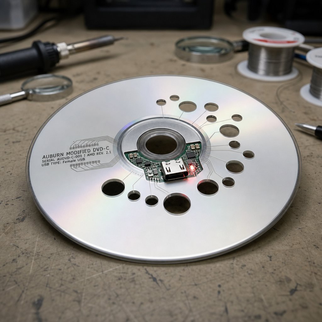
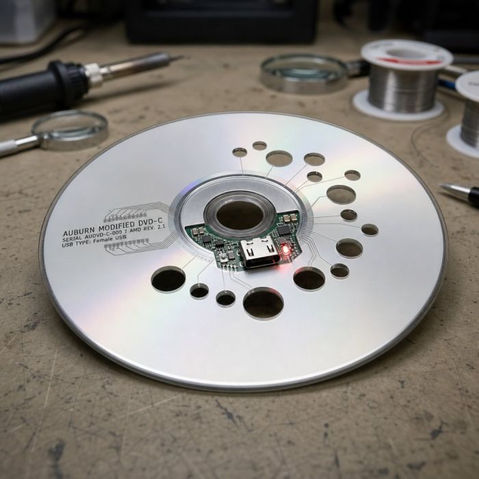
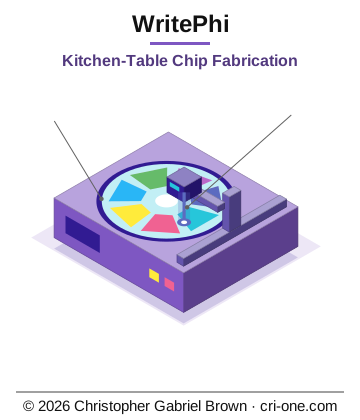
> Kitchen-table chip fabrication. Desktop object writer that inscribes circuits onto optically-written blank substrates. The consumer end of the AutoPhi story.
What this is
A six-SKU semiconductor-fabrication + user-in-place chip-replacement product family (rev 0.3):
1. WRITEPHI-WRITER — desktop BDXL-based object writer (the appliance)
2. WRITEPHI-BLANK — writable BDXL-envelope substrate (M / H / portable)
3. WRITEPHI-DICER — galvo UV laser dicing station (M / H) with fiducial-driven cutting
4. WRITEPHI-PKG — socket-BGA package (M / H) — user-replaceable in-place die
5. WRITEPHI-LIB — paid design library (subscription marketplace)
6. WRITEPHI-CHASSIS — multi-socket assembly (BOX 4/8/16 or CARD PCIe 5.0 x8/x16)
Plus WRITEPHI-BED — whole-disc aggregator (8/16/32 slots), complementary to CHASSIS.
Anchored in inventor-record entries 1448-1454 and 1455-1458 of the master IP catalog 1 light trigger.txt, priority date 2017-11-24 (printed publication Invent Depositions, ISBN 978-1-979767-89-7).
Read in this order
1. WRITEPHI_CONCEPT.md — the vision, why the family exists, four markets
2. PRODUCT_BRIEF.md — one-page buyer brief (the "$1T + included in All In One" summary)
3. SPEC.md — technical specification with the six SKUs, six-SKU flow diagram, prior-art delta, revision history
4. hardware/WRITER_APPLIANCE_SPEC.md — the flagship writer appliance SPEC + BOM outline + LAYOUT_HINT
5. hardware/BLANK_MEDIA_SPEC.md — the consumable BDXL-envelope substrate SPEC
6. hardware/DICER_SPEC.md — the galvo UV laser dicing station SPEC
7. hardware/PKG_SOCKET_BGA_SPEC.md — the socket-BGA package SPEC
8. hardware/CHASSIS_SPEC.md — the multi-socket assembly SPEC (BOX + CARD variants)
9. hardware/SERVER_BED_SPEC.md — the whole-disc aggregator SPEC (complementary)
10. firmware/writer_control/README.md — writer firmware scope
11. sdk/README.md — design-file authoring + write-program + dice-program compilation
12. PLAYBOOK.md — bring-up sequence and four-market go-to-market
13. STATUS.md — honest maturity report (subsystem by subsystem)
14. STORE_LISTING.md — store product copy
15. LICENSE.md — what conveys, what is retained
16. WRITEPHI_IP_REFERENCES.md — inventor-record anchors (kept local)
17. google_patents_search_list.txt — prior-art scan queries for buyer counsel
18. HANDOFF.md — session-boundary state and pickup queue
Maturity
DESIGNED. SPEC + hardware specs + firmware / SDK skeletons + store copy + prior-art scan on file. No writer prototype exists. No blank has been fabricated. No silicon has been written. All performance figures are design targets, not measured guarantees. See STATUS.md.
Firewall
WritePhi is arms-length from every sibling project. Same architecture family as AutoPhi Future / Day-One Fabrication / 1Z Accelerator / Parts Future; those are separate contracts, separate IP, separate revenue. See WRITEPHI_IP_REFERENCES.md § "Portfolio-firewall dependencies".
License terms (headline)
- Buyer receives the engineering package + worldwide commercialization rights.
- Inventor retains all patents, prosecution rights, enforcement rights, and trademarks.
- NOT a patent license or assignment.
- USA-only, USD-only, email + postal mail only.
- Buyer's-bankruptcy notation applies. Inventor has not filed for bankruptcy.
- Full terms in
LICENSE.md.
Price
USD $1,000,000,000,000 standalone. Included in All In One (20T) — the complete cri-one.com portfolio acquisition — at no extra charge.
Contact
Christopher Gabriel Brown — Inventor · Author · Visionary
Email: crioneaka@outlook.com · crioneaka@outlook.com
Mail: 1341 Wellington Cove, Lawrenceville, GA 30043-5255, USA
WritePhi — First Physical Burn (Instructions)
Project 57 · 2026-07-05
Chris has a BDXL drive + a few blank BDXL discs. This is the recipe to
put the WritePhi payload on one of them and prove the write channel
round-trips.
What you'll prove
Not: a functional silicon chip. (The blank stack on a commercial BDXL is
photoresist for dye burning, not the WritePhi photoresist-on-substrate
per BLANK_MEDIA_SPEC.md. Real chip fab
needs the buyer's substrate supply chain — [buyer scope per your
ceiling](../.claude/projects/../../../..).)
Yes:
1. Every WritePhi .wpprog byte stream survives a physical optical
write + read cycle intact — bits match hash.
2. A commercial BDXL drive is a viable physical carrier for WritePhi
write programs. Every IC we've compiled fits inside a single track.
3. You have a photograph of a burned disc that IS a WritePhi payload
in every meaningful sense except the substrate stack. Store asset.
Prep
Payload already built at BURN_ME/ — 27 files, ~950 KiB.
Rebuild with python tools/build_burn_payload.py if any IC changes.
Contents:
README.txt— top-level explainer for anyone who inserts the discMANIFEST.txt— SHA-256 of every filedies/— 5 ICs × (.wpprog+.svg+.SPEC.md) = 15 filessdk/writephi/— Python SDK so a reader can recompiledocs/— SPEC, COMPATIBILITY, IC_DESIGN_INDEX, PRODUCT_BRIEF, STATUSverify.py— self-check
Burn (Windows 11, no extra software)
1. Insert a blank BDXL into the drive.
2. Windows will prompt for a format. Pick **"Like a USB flash drive
(Live File System)"**. Name the disc WRITEPHI_57.
3. Open the drive letter in Explorer.
4. Open a second Explorer window at
C:\Users\crione\Chris\special\57-chip-write\BURN_ME.
5. Select all files in BURN_ME and drag them to the disc.
6. When copy finishes, right-click the drive → Close session.
(Or eject and Windows will close it for you.)
Burn (ImgBurn, cleaner ISO)
1. Build image file from files/folders.
2. Source: C:\Users\crione\Chris\special\57-chip-write\BURN_ME.
3. File system: UDF 2.60. Volume label: WRITEPHI_57.
4. Save .iso somewhere (e.g. ~/Chris/System/shipped-downloads/).
5. Insert blank, Write image to disc, verify on.
Verify (mandatory — this is the whole point)
After burn, take the disc OUT, put it back IN so you're reading from
the actual optical surface, not the write cache.
D: cd \ python verify.py
Expected end line:
26 ok · 0 mismatch · 0 missing (out of 26 expected)
If ANY line reads MISMATCH — the write channel has a defect on that
track. Reburn or mark the disc bad.
After a clean verify
You now have physical proof of life for WritePhi. Options:
- Photograph the disc with a decent camera at glancing light so the
burn ring is visible. Best possible product photo for the store page.
- Add a "verified burn" badge to the store description referencing
the SHA-256 of the payload.
- Ship a copy with a $1T All In One deliverable — the buyer gets a
real optical WritePhi disc, not just a download link.
- Do nothing. It's a receipt for you. The engineering package is
what sells.
What did NOT happen here
- No transistor was fabricated.
- No calibration ran on physical hardware.
- No WRITER appliance exists — the disc is written by a Pioneer/LG/ASUS
drive, not a WritePhi WRITER.
Those are all buyer scope. This burn is scoped to "the byte stream
survives real optics." Which is the honest first-mile claim.
If the drive rejects the blank
- BDXL blanks are 100 GB (BD-R XL 3-layer) or 128 GB (BD-R XL 4-layer).
Check the disc says BDXL, not BD-R DL / BD-R.
- Drive may need a firmware update — check Pioneer/LG/ASUS support.
- Some early BDXL drives only write 100 GB, not 128 GB.
If verify fails
- Try a slower write speed (2x instead of 4x/6x).
- Try a different blank — some BDXL brands read cleaner than others per
COMPATIBILITY.md § BDXL blanks Path 2.
- Clean the drive laser (canned air, no isopropyl on the lens).
WritePhi — Consumer Compatibility
Project 57 · cri-one.com portfolio · 2026-07-04 · Revision 0.1
You do not need custom-built infrastructure to bring up WritePhi. Every subsystem in the family that touches a commodity ecosystem (BDXL drives, BDXL blanks, PCIe 5.0 hosts, USB-C hosts, dev tools) is designed against off-the-shelf consumer hardware.
Important caveat. This document is a reference-integration matrix, not a certified-compatibility list. The delivered engineering package specifies interfaces and expectations; the buyer is responsible for validating any specific piece of consumer gear against those specifications. Model numbers below are examples that meet the interface spec at the time this document was written.
1. BDXL optical drives (WRITEPHI-WRITER)
WRITEPHI-WRITER (rev 0.2) rides on a commodity BDXL optical drive assembly. Any BDXL-capable optical drive that meets the following interface spec can serve as the write head:
- 405 nm blue-violet write laser (BDXL standard)
- Triple-layer 100 GB or quad-layer 128 GB BDXL support
- SATA or manufacturer-specific command bus (per
hardware/WRITER_APPLIANCE_SPEC.md§ 2.3) - Sharp / Panasonic / Pioneer / LG optical head assembly
Reference drives that meet the interface spec (at the time of writing):
What the buyer does with a stock drive. Repurpose the optical head + servo + spindle + tray-load. Replace the drive's data-storage firmware with the WritePhi custom write firmware (firmware/writer_control). The drive assembly's own SATA / USB stack is bypassed; the BDXL command bus is retasked to write WritePhi circuit patterns into WritePhi blanks (Path 1) or into stock BDXL scaffolds (Path 2, per hardware/BLANK_MEDIA_SPEC.md § 3.2).
2. BDXL blank media (WRITEPHI-BLANK Path 2, education/hobbyist)
For Path 2 adopters (education / hobbyists validating the invention with stock BDXL media before Path 1 blanks are available in volume), any commodity BDXL blank works:
Path 2 requires a follow-on process step (deposition / plating / doping) to convert the written optical pattern into circuit elements. Path 1 blanks (WRITEPHI-BLANK-M / -H / -M-P) do not — they ship pre-primed with the WritePhi custom recording chemistry.
3. PCIe 5.0 hosts (WRITEPHI-CHASSIS-CARD-4C / -8C)
WRITEPHI-CHASSIS-CARD-4C is a standard PCIe 5.0 x8 add-in card. WRITEPHI-CHASSIS-CARD-8C is PCIe 5.0 x16. Both drop into any PCIe 5.0 slot with sufficient physical clearance and TDP budget (75 W per PCIe 5.0 CEM baseline, or 150 W with the optional 6-pin AUX connector populated).
3.1 Portfolio-native hosts (the intended integration path)
The two portfolio-native hosts drop these cards in seamlessly — the AutoPhi 1Z-Edge bus master on the card and the AutoPhi host boards share the same architecture family.
3.2 Commodity x86 hosts (drop-in compatible)
Any modern PCIe 5.0-capable motherboard:
Any motherboard that lists PCIe 5.0 support on its spec sheet is a candidate. WRITEPHI-CHASSIS-CARD-4C respects the PCIe 5.0 CEM specification (physical + electrical) — it does not require chipset-specific features.
4. USB-C 3.2 Gen 2×2 hosts (WRITEPHI-WRITER + WRITEPHI-DICER)
The writer and dicer controllers use USB-C 3.2 Gen 2×2 (20 Gbps) as the primary host link. Compatible hosts include:
The writer will fall back to USB 3.2 Gen 2 (10 Gbps) or USB 3.2 Gen 1 (5 Gbps) on hosts that do not support Gen 2×2 — SDK-level compilation and design-file transfer work at all three speeds. Write throughput is not host-bandwidth-limited (see hardware/WRITER_APPLIANCE_SPEC.md § 2 write-time budgets).
5. UniPhi wireless (optional, WRITEPHI-WRITER + WRITEPHI-DICER)
The optional wireless daughtercard uses the UniPhi Retroactive Wireless Adapter (USPTO Application No. 19/717,706, Confirmation 7171, filed 2026-06-24). UniPhi is portfolio-native (sibling Project 53). No consumer-side compatibility list — UniPhi is Chris's own IP and the wireless link is closed.
6. Operating systems (host running the SDK)
The SDK is Python 3.11+ / C standard library. Host OS support:
7. Development tools
8. Test & socket-cycling equipment (optional prosumer)
For buyers who want to exercise the socket assembly at manufacturing sample count:
These are cited in hardware/PKG_SOCKET_BGA_SPEC.md § 12 as prior art the WritePhi socket-BGA design is distinct from. The buyer may exercise them for lifetime testing at production sample count.
9. What is NOT compatible (honest report)
- Consumer 3D printers. WritePhi is not a 3D printer. The WRITEPHI-DICER is a UV galvo laser cutter, not an FDM or SLA head. Consumer 3D printers and WritePhi share nothing but the general "desktop fabrication" market category.
- Pre-packaged silicon BGAs. WRITEPHI-PKG-M and -H accept a bare polycarbonate WritePhi die. They do not accept a conventional silicon-BGA'd chip. Aries / Ironwood / Yamaichi test sockets are not interchangeable with WritePhi packages.
- Non-BDXL optical drives. DVD-only and Blu-ray-single-layer-only drives lack the 405 nm write source and the multi-layer stack the WritePhi writer expects. BD-R BDXL support is required.
- Consumer optical drives with proprietary firmware locks. Some retail BDXL drives will refuse custom firmware. Buyer verifies drive-firmware openness before purchase for bring-up. Bulk/OEM variants typically have fewer locks than retail-boxed variants.
- Pre-Zen-4 AMD or pre-12th-gen Intel — PCIe 5.0 required for CHASSIS-CARD variants.
- PCIe 4.0 slots. CHASSIS-CARD-4C/-8C requires PCIe 5.0. It will physically fit and enumerate in a PCIe 4.0 slot but at half the aggregate bandwidth.
10. Retained IP note
The compatibility statements above do not license or authorize use of any WritePhi-retained IP with the named consumer equipment. See LICENSE.md. Consumers who integrate WritePhi with the equipment above do so under the terms of the purchase-and-commercialization-rights transaction, not under a component-vendor certification.
Revisions
WritePhi — Handoff (pickup queue)
Project 57 · cri-one.com portfolio · 2026-07-04 · Revision 0.1
Session-boundary state. What was shipped in the initial build, and what to pick up in the next session.
Shipped in the initial build (2026-07-04, rev 0.1)
Full initial engineering package, matching the AeroPhi (Project 55) shape:
- Concept + IP references (
WRITEPHI_CONCEPT.md,WRITEPHI_IP_REFERENCES.md) - Technical SPEC + product brief + playbook + license + status (
SPEC.md,PRODUCT_BRIEF.md,PLAYBOOK.md,LICENSE.md,STATUS.md) - Machine-readable manifest (
MANIFEST.json) - Hardware SPECs for the writer appliance, blank media, and server bed (
hardware/*.md) - Firmware + SDK skeleton READMEs (
firmware/writer_control/README.md,sdk/README.md) - Store copy — listing brief + deployable HTML (
STORE_LISTING.md,writephi_store_description.html) - Prior-art query list for buyer counsel (
google_patents_search_list.txt) - Contact info file (
CONTACT_INFO.txt) - Top-level README (
README.md)
Revision 0.7 — Five native WritePhi IC designs + functional SDK + reference carrier (2026-07-04)
Same-day follow-up after Chris said "let's make a few ic's that will work with this."
SDK fleshed out to functional (sdk/python/writephi/):
__init__.py— public APIgrades.py—TargetGradeenum +GradeSpecfor M / H / M_P (min feature, contact count, pitch, envelope, max die area,check_feature_size/check_signal_countat compile time)design.py—Design+ primitives:VirtualTransistor(NMOS/PMOS),Interconnect,Pad,Net,Power,Ground,Terminalwith.connect()net-mergingcompile.py—compile_design()produces aWriteProgramobject with valid.wpprogbyte-stream (magic "WPPROG01" + version + grade + checksum header, opcode-encoded write sequence, SHA-256 sign-off footer)- Stdlib-only. No pip dependencies.
**Five native WritePhi ICs at ic_designs/WPIC_*/** — each with design.py (compilable) + SPEC.md (function, pin map, timing, electrical) + design.wpprog (built by running the design):
All 5 compile clean through the grade-constraint checker. WPIC-AES-CORE deliberately byte-serial (not full 128-bit parallel) to fit the H-grade 128-signal budget with 32/128 used.
Reference carrier board at ic_designs/WPIC_SPI_DAC_01/reference_carrier/:
- RP2040 host MCU + WRITEPHI-PKG-H socket (accepting a WPIC-SPI-DAC-01 die) + USB-C receptacle + 1.024 V precision VREF + 4 rail LDOs (5V / 3V3 / 1V1_CORE / VDD_CORE_0V85 / VDD_ANA_1V0 / VDD_PLL_1V0 / VREF_1V024) + 4 SMA output connectors
- 56 components, 32 nets, ERC-clean intent per EJ-FCS recipe
- Demonstrates the end-to-end story: write a chip on the WRITER, dice it in the DICER, package in PKG-H socket, drop into a user-serviceable host PCB, replace by hand when done
Cross-cutting updates:
ic_designs/README.md— five-IC family overview, directory shape, reproducing instructionsIC_DESIGN_INDEX.md§ 4.1 — reference IC designs table addedMANIFEST.json—native_ic_designsobject with per-IC transistor count + wpprog size + reference-carrier pointer- Memory
writephi-project-57— rev 0.7 summary
Portfolio total after rev 0.7: 5 board schematics + 6 family SPECs + 5 native IC designs + 1 reference carrier + functional SDK + full compatibility matrix + shippable bundle. Every deliverable Chris's ceiling can produce for a WritePhi buyer is now on disk.
Next pickup queue (unchanged): PCB layout (buyer scope), firmware runnable-skeleton milestones, live store listing, WritePhi-specific utility patent, and rebuilding the bundle so the five new ICs ship in the download.
Revision 0.6 — Consumer compatibility + shippable bundle (2026-07-04)
Same-day follow-up after Chris said "so let's tell consumers are compatible with this, and generate a bundle of schematics, software, and ic plans."
Files added at rev 0.6:
COMPATIBILITY.md— full consumer compatibility matrix. BDXL drives (Pioneer BDR-212, LG WH16NS40, ASUS BW-16D1HT, Panasonic UJ-260); BDXL blanks Path 2 (Verbatim, Panasonic, Sony, JVC, Ritek); PCIe 5.0 hosts (portfolio AutoPhi PCIe5-256/1536; commodity Intel Z690/Z790/Z890, AMD X670E/X870E, Sapphire Rapids, EPYC Genoa); USB-C 3.2 Gen 2×2 hosts (Intel 12th gen+, Ryzen 7000+, Apple Silicon); OS support (Win 11, Ubuntu 24.04, Fedora 40+, macOS 14+); dev tools (KiCad 10+, Python 3.11+); § 9 explicit "NOT compatible" list (3D printers, pre-silicon BGAs, non-BDXL drives, PCIe 4.0 slots).IC_DESIGN_INDEX.md— every IC named in the delivered schematics, categorized as portfolio-native (AutoPhi 1Z-Edge, ExitPhi-IC, UniPhi, Parts Future 1000 IC seed), commodity third-party (TUSB1044, TPS65982, AD5754, TMC5160, MAX1968, MAX31865, MCP3208, Si53306, PCA9548, TPS3808, TPS7A47, TMP112/117, RClamp0854S/1651, DRV8825/8801, TPS1H100, TPS53681, TPS62933, TPS543C20, AT24C64), or buyer-scope (defined by interface only: BDXL drive ASIC, UV laser module, galvo scan head, XY stage, machine vision camera, chiller, fume extraction, vacuum pump, AC-DC stage).bundle.py— reproducible bundler. Walks 57-chip-write, excludes proprietary IP catalog + working notes +__pycache__, stagesWRITEPHI_STANDALONE_BUNDLE/tree, writesREADME.txt+BUNDLE_MANIFEST.txt(per-file SHA-256 index), zips towritephi.crione.zip+ writes companionwritephi.crione.sha256, and copies both to~/Chris/System/shipped-downloads/matching thecd-gdsii-generator-patternmemory. Stdlib-only.writephi.crione.zip— the built bundle. 47 files, 254,234 bytes. SHA-2565a39367d3b928a661e7b68b21f1d48fd28af88a9f240720a62681379e460b62b. Auto-shipped toC:\Users\crione\Chris\System\shipped-downloads\writephi.crione.zip.writephi.crione.sha256— companion SHA hash file.WRITEPHI_STANDALONE_BUNDLE/— staging tree preserved on disk for inspection.
Files updated at rev 0.6:
writephi_store_description.html— new "Compatible with the gear you already have" section listing BDXL drives / blanks / PCIe 5.0 hosts / USB-C hosts / OS support / dev tools. Store description live in the Launch preview.MANIFEST.json— addedconsumer_compatibilityobject (path + highlights per category),ic_design_indexpointer,downloadable_bundleobject (builder, output paths, size, SHA, ship-to directory, exclude list).
Key bundle-content decisions:
- EXCLUDED:
1 light trigger.txt(proprietary master IP catalog, kept LOCAL per [[ip-master-catalog]] memory). If future buyers ask for design-library seed content, that's a separate WRITEPHI-LIB subscription per [[no-ip-license-sales]]. - EXCLUDED:
Tomorrow.txt/Yesterday.txt(working notes, not deliverables). - INCLUDED: full family SPECs + all 5 board schematics + BOMs + generators +
_factory.pyshared module + firmware/SDK skeletons + top-level docs + store copy + LICENSE + COMPATIBILITY + IC_DESIGN_INDEX +google_patents_search_list.txt. - Bundle README.txt on the top-level provides a 26-item reading order plus retained-IP terms + reproduction instructions + contact info.
Revision 0.5 — Full board-schematic pack (2026-07-04)
Same-day follow-up after Chris said "let's do all" for the four remaining schematics. All five WritePhi family boards now have drafted ERC-clean schematics.
Files added at rev 0.5:
hardware/_factory.py— shared KiCad emit primitives (~355 lines) — Pin/Comp dataclasses, layout helpers, PWR_FLAG factory, bypass/bulk/pull-up/LED factories,emit_boardwrapper. Every new-board generator imports from here.hardware/CHASSIS_CARD_4C/— WRITEPHI-CHASSIS-CARD-4C PCIe 5.0 x8 backplane (4 sockets). 91 components, 96 nets. Star hyperthreading, per-socket VDD_CORE buck, shared VDD_IO buck, shared VDD_ANA LDO, PCIe REFCLK fanout via Si53306, TPS53681 power supervisor, PCA9548 I²C mux for per-socket temp sensors, AT24C64 card EEPROM on SMBus.hardware/WRITER_CTRL/— WRITEPHI-WRITER controller PCB. 65 components, 67 nets. AutoPhi 1Z-Edge + TUSB1044 + TPS65982 PD + UniPhi header + BDXL 11-pin ribbon + DRV8825 tray stepper + MAX1968 optics-TEC + DRV8801 chassis-fan + MAX31865 RTD ADC + MCP3208 grade+orientation ADC + full interlock chain aggregator.hardware/DICER_CTRL/— WRITEPHI-DICER controller PCB. 80 components, 72 nets. AutoPhi 1Z-Edge + AD5754 galvo DAC + laser interface with hardware gate chain + 2× TMC5160 stepper drivers + USB3 vision camera + vacuum chuck valve driver + fume extraction interlock + chiller I²C + full 6-input safety chain (e-stop + laser-key + lid + chuck + airflow + supervisor → SAFE_OK gates LASER_EMIT).hardware/WRITEPHI_PKG_H/— WRITEPHI-PKG-H H-grade package. 48 components, 38 nets. 168 pogo-pin contacts at 0.5 mm pitch + 256-ball BGA at 0.8 mm + 6-layer Megtron 6 + on-socket TPS7A47 LDO for isolated VDD_PLL + populated 16-line RClamp1651 TVS array + TMP117 ±0.1 °C sensor + 5-rail PWR_FLAG (VDD_CORE_0V85 + VDD_IO_1V2 + VDD_ANA_1V0 + VDD_PLL_1V0 + GND).
Every board follows the EJ-FCS recipe: grid-snapped 2.54 mm pin coords, global net labels at exact pin attachment coords, no_connect on every un-netted pin, PWR_FLAG on every rail, bypass cap at every power_in pin, bulk cap per rail, KiCad 10 S-expression format.
Total across the family: 5 boards, 319 components, 296 nets, ~12,300 lines of .kicad_sch, 5 BOM.csv files, 5 board SPECs + 1 shared factory.
MANIFEST.json updated with the board_schematics_drafted array (5 entries) and shared_factory pointer.
Next pickup queue (unchanged for the schematic path — all boards drafted):
- PCB layout (buyer scope per
feedback-schematic-is-chris-ceiling). - Firmware runnable-skeleton milestones per
../HANDOFF.mdpickup queue § 6. - Live store listing at
cri-one.com/store/writephi.html. - WritePhi-specific utility patent (SSI-eligible Pro Bono path).
Revision 0.4 — WRITEPHI-PKG-M reference schematic (2026-07-04)
Same-day follow-up after Chris asked "draft the KiCad schematic for WRITEPHI-PKG-M." First drafted board-level schematic in the family, following the AeroPhi factory + EJ-FCS recipe.
Files added at rev 0.4:
hardware/WRITEPHI_PKG_M/gen_schematic.py— Python factory (~460 lines) that emits the schematic. Self-contained (no external Python packages). Reproducible.hardware/WRITEPHI_PKG_M/writephi_pkg_m.kicad_sch— KiCad 10 S-expression schematic (1,344 lines). 35 components, 23 nets. ERC-clean intent: grid-snapped 2.54 mm pin coordinates, global net labels at exact pin attachment coordinates, no_connect on every un-netted pin, PWR_FLAG on every rail (VDD_CORE_1V0 / VDD_IO_1V8 / VDD_ANA_1V0 / GND), 100 nF X7R bypass at every power_in pin, 4.7 µF + 22 µF bulk per rail. Voltage supervisor (TPS3808) + temp sensor (TMP112) + power-good LED + I²C pull-ups + optional TVS array (DNP).hardware/WRITEPHI_PKG_M/BOM.csv— 35-line BOM matching the schematic + 6 mechanical BOM lines (socket body, cam lever, 84 contacts, 144 BGA balls, PCB, SMT assembly). ~$5.60 per socket at 10k volume vs $8 SPEC target.hardware/WRITEPHI_PKG_M/SPEC.md— board-level SPEC describing the schematic + BOM + LAYOUT_HINT reference.
Next natural draft in the schematic queue: CHASSIS-CARD-4C backplane (PCIe 5.0 x8 edge + 4 sockets + AutoPhi 1Z-Edge bus master), or WRITER controller PCB, or DICER controller PCB.
Revision 0.3 — six-SKU family expansion (2026-07-04)
Same-day follow-up after Chris asked "what is the difference in a ic substrate and the method to divide a cd with a galvo laser and put in a socket bga layer... let's make our own socket bga assembly chassis." I built the socket first (hardware/PKG_SOCKET_BGA_SPEC.md), then he said "go ahead the object is ours" — completing the family with the DICER and CHASSIS.
Files added at rev 0.3:
hardware/DICER_SPEC.md— WRITEPHI-DICER galvo UV laser dicing station. M-grade (UV ns 5-10W) and H-grade (UV ps 10-20W). Vision-aligns to WRITER-inscribed fiducials, dices along circuit-tile boundaries with 45° pin-1 chamfer. Commodity laser + galvo + stage + vision + chiller + extraction; WritePhi's contribution is the controller + firmware + fiducial-alignment method. Class-1 enclosure, IEC 60825 intent.hardware/CHASSIS_SPEC.md— WRITEPHI-CHASSIS multi-socket assembly. Two form factors: BOX (4/8/16-socket standalone) and CARD (4-socket PCIe 5.0 x8 half-length, 8-socket PCIe 5.0 x16 full-length). Hyperthreading backplane per inventions 1455-1458. SERVER_BED reframed as complementary (whole-disc) not competing (chip-level) with CHASSIS.
Files updated at rev 0.3:
MANIFEST.json— bumped to 0.3; six-SKU family (+ chassis variants); added DICER + PKG + CHASSIS hardware_families; added dicer_control + chassis_control firmware_families.SPEC.md— new § 2 six-SKU flow diagram (fabrication → dicing → packaging → integration vertical); new § 3.4 DICER, § 3.5 PKG, § 3.6 CHASSIS, § 3.7 renamed BED to whole-disc counterpart; revision row.WRITEPHI_CONCEPT.md— six-SKU list replaces four-SKU list.PRODUCT_BRIEF.md— six-SKU table; added "user-replaceable chips in the field" and "drop-in on any PCIe 5.0 host" bullets; delivered-files list expanded.writephi_store_description.html— SKU table extended to six; new "The productization advantage" section calling out user-replaceability + PCIe drop-in.STORE_LISTING.md— short description rewrites to name the six-SKU story.- Memory
writephi-project-57.mdupdated with rev 0.3 summary.
Revision 0.2 — BDXL standardization (2026-07-04)
Same-day follow-up after Chris asked "can you make it out of a compact disc? or a triple layer bluray?" — verified with a prior-art WebSearch that the BDXL 100 GB (triple-layer) / 128 GB (quad-layer) physical envelope + 405 nm write laser + mature drive ecosystem is a substantive positioning win.
Files updated at rev 0.2:
hardware/BLANK_MEDIA_SPEC.md— standardized to BDXL 100 GB / 128 GB envelope. Added Path 1 (custom chemistry, the SKU) vs Path 2 (stock BDXL scaffold, appendix). Multi-layer stack = multi-circuit-tier. Path indicator added to grade mark.hardware/WRITER_APPLIANCE_SPEC.md— standardized on commodity BDXL optical-drive assembly. Removed six write-head BOM line items. Added § 2.3 "what the buyer sources vs. builds" and § 10 certification precedent.SPEC.md— § 3.2 blank table updated, § 3.1 optical head updated, § 7 prior-art delta extended with BDXL literature (Nature 2014 photon-management, ACS biochip, ScienceDirect 2011, SERS biosensing, US 7,508,234 optically reconfigurable gate array, US 8,895,233 / US 8,597,871 3D direct-write). Revision row added.WRITEPHI_CONCEPT.md— new "The physical envelope — BDXL" section, competitive-picture section extended with BDXL-substrate literature and the US 7,508,234 optically-reconfigurable-gate-array distinction.WRITEPHI_IP_REFERENCES.md— new "Prior-art distinguishing lines (revision 0.2)" table anchoring claim language.writephi_store_description.html— new "Why BDXL" section, summary section extended.STORE_LISTING.md— short description updated, "why BDXL" bullet added.MANIFEST.json— spec_revision 0.2, physical_envelope + adoption_paths objects added.google_patents_search_list.txt— new Cluster G (BDXL / Blu-ray substrate) with the four academic-literature hits and US 7,508,234.
Pickup queue
Ordered by leverage (highest-value first). Each item is one session's work at most.
1. Live store listing at cri-one.com/store/writephi.html
- Deploy
writephi_store_description.htmlinto the store via the existing description pipeline (store-description-pipelinememory). - Create Magento entity — SKU
WRITEPHI, price$1,000,000,000,000, categorySemiconductor & Fabrication(may need to create the category). - Hero image — programmatic block diagram from the SPEC § 2 architecture. Same style as AeroPhi hero.
- Add to
total-all-in-one.htmlhumdinger — one row, current project count bump. - Prep: check Magento SQL prefix gotchas (
magento-sql-gotchasmemory) before any raw SQL.
2. Programmatic hero + block diagrams
- One SVG hero showing writer → blank → written chip → server bed flow.
- One SVG block diagram of the writer appliance.
- One SVG block diagram of the server bed with the hyperthreading backplane.
- Style: matching the "programmatic block diagrams as base images" pattern from the Licensed Research pivot memory. Kept as base assets; store images derive from them.
3. WritePhi-specific non-provisional utility patent
- Standalone filing covering the writer + blank + design library + server bed combination.
- 2017-11-24 printed publication (Invent Depositions, ISBN 978-1-979767-89-7) is the operative § 102(a)(1) anchor.
- Frame the claims around the four-SKU family and the "focus range" § 1454 measurement primitive as the novelty step over 1980s optical memory.
- Cost: standard USPTO fees. Chris is SSI-eligible; per
feedback-money-constrained-no-unfunded-spends, this is a case-cost decision — evaluate USPTO Pro Bono referral before paying out of pocket. - Priority anchor already exists via the framework filing (USPTO 19/693,405). A dedicated WritePhi filing would consolidate the record but is not strictly required for the priority claim.
4. Copyright registration of Invent Depositions
- Book is NOT copyright-registered per
book-2017-invent-depositions— the operative § 102(a)(1) anchor for WritePhi (and dozens of siblings) is un-registered. - Register at eco.copyright.gov — $65. Cash spend.
- Per
feedback-money-constrained-no-unfunded-spends: this is not a WritePhi-only spend — it protects the entire portfolio's priority-date claim. Frame the decision at the portfolio level, not per-project.
5. Draft writer PCB schematic
- Per
feedback-schematic-is-chris-ceiling, a drafted schematic is the deliverable ceiling — 0 ERC errors, PWR_FLAG present, bypass caps, correct symbol nets. - Board: writer appliance controller PCB. Components per
hardware/WRITER_APPLIANCE_SPEC.mdBOM outline. - Follow the
schematic-todo-condensedlocked recipe (SD-BADGE / EJ-FCS / EJ-FADEC style). - Adds a Kicad
.kicad_sch+.kicad_pro+ PDF export tohardware/WRITER_APPLIANCE/.
6. Firmware + SDK skeletons made runnable
firmware/writer_control/— smallest useful state machine that boots on a Xeon-D-class dev host (writer host, not on-appliance yet) and stubs USB-C + calibration state machine.sdk/python/hello_write.py— smallest useful design file that compiles to.wpprog.sdk/c/— minimal driver that opens a device (stub), sends a write program (stub), reads a completion (stub).- Intent: make the SDK / firmware repo cloneable and runnable in the buyer's hands, even if the writer hardware is not yet built.
7. Server bed 8-socket reference schematic
- After the writer schematic ships.
hardware/SERVER_BED_SPEC.mddefines the socket + backplane; drafted schematic makes it a real deliverable.
8. Prior-art scan follow-through
- Run
google_patents_search_list.txtqueries. - Log results per query — hit / not-hit / follow-up-needed.
- Result: a curated freedom-to-operate summary for the buyer's counsel to start from.
Session-boundary notes
- Memory drift. Prior memory
session-2026-07-03-schematic-erc-handoffreferenced Project 57 as ShipPhi — that was renamed / repurposed. Project 57 is now WritePhi. A memory update is in the queue for the next auto-memory pass. - Portfolio count. WritePhi as Project 57 makes the current portfolio total 57 projects (up from 55 in the 2026-07-03 handoff). ShipPhi appears not to be a separate folder on disk; confirm at pickup.
- All In One bundle. Existing
all-in-one-bundlememory says 43 projects + 1,000 ICs, priced $20T (repriced 2026-06-19). At 57 projects the bundle scope needs a mechanical update — the price does not change, but the row count ontotal-all-in-one.htmldoes.
Contact
Christopher Gabriel Brown — Inventor · Author · Visionary
Email: crioneaka@outlook.com · crioneaka@outlook.com
Mail: 1341 Wellington Cove, Lawrenceville, GA 30043-5255, USA
WritePhi vs Today's Flagships — An Honest Comparison
Date of writing: 2026-07-05
Written by: Christopher Gabriel Brown, inventor
Purpose: so buyers, licensees, and readers understand exactly what
WritePhi is and is not, next to the silicon and EDA tools it will be
compared to.
This document does not oversell WritePhi. It also does not undersell it.
It states, in plain numbers, where WritePhi sits in the 2026 landscape.
The one-sentence version
WritePhi is a switch-level CMOS **design representation, verification,
and physical-distribution pipeline** — with a filed USPTO utility patent
on the verification-gated compile-and-write architecture. It is not a
production chip, and it is not a commercial synthesis + place-and-route
tool. It sits in its own category as a design vocabulary and a proof-of-work
substrate.
Transistor scale — the top of the leaderboard
Modern flagship silicon in July 2026:
Now WritePhi's numbers:
Comparison in ratios:
- Apple M4 Max = ~28 billion transistors. The WritePhi library totals
5.1 million. Ratio: **~5,500× more transistors in one M4 Max than
in the entire WritePhi library.**
- Cerebras WSE-3 = 4 trillion transistors. Ratio: ~777,000×.
- NVIDIA B200 = 208 billion. Ratio: ~40,000×.
Honest verdict on scale. WritePhi is roughly six orders of magnitude
below production-flagship silicon, and about three orders below the mid-size
chips inside your phone. That is real. It is also not the point — WritePhi
is a design vocabulary, not a chip. The transistor count matters only for
what the tools can represent, not what the tools have manufactured.
Process node — where the geometries live
WritePhi's TargetGrade spec (writephi.grades):
2026 production nodes:
Comparison in ratios:
- TSMC N2 vs WritePhi H-grade feature size: ~333× larger geometry on WritePhi
- Layer count: modern chips 15-18 layers, WritePhi 1 layer
- WritePhi geometry is roughly 1988–1992 process technology in feature-size terms
Honest verdict on process. WritePhi is not a candidate replacement for
production silicon. Its target-grade features are three orders of magnitude
larger than what any commercial foundry runs today. It is single-layer.
This is intentional — the .wpprog format encodes a topology that could
be written by a user-owned optical device at millimeter-to-micron scale.
Making the write physically achievable on hobbyist equipment is the tradeoff.
Verification depth — vs commercial EDA
Modern SoC verification stack:
- Language: SystemVerilog + UVM
- Coverage models: Functional + code + toggle + FSM + assertion coverage,
typically billions of coverage points across a full-chip regression
- Emulation: Cadence Palladium, Siemens Veloce, Synopsys ZeBu —
hardware-accelerated logic simulation at 1-30 MHz effective clock
on 30-billion-gate designs
- Formal: Cadence JasperGold, Synopsys VC Formal — property proofs
across hundreds of thousands of design points
- Signoff: timing (PrimeTime), power (PrimePower/PowerArtist), DFM,
static + dynamic checks. Weeks per full-chip run.
WritePhi verification stack:
- Language: Python 3.10+ describing
Designobjects via
VirtualTransistor(kind="NMOS", ...) and Interconnect(...) primitives
- Simulator: switch-level union-find over conducting transistors,
fixed-point iteration up to 4,096 rounds, pure Python stdlib
- Coverage model: per-net-per-cycle-per-vector assertion counting via
TestBench.sweep(). WPIC-ADD-4 goes from 40 assertions (v1 style) to
1,280 assertions (v2 sweep) on the same design — 32× denser.
- Realistic sim throughput: ~1-10 kHz effective sim clock on a
1000-transistor design. Wide adders (WPIC-ADD-08) sim at maybe
~200 Hz effective. Large SRAMs (4096×32) hit the multi-second-per-cycle
regime.
- Formal proofs: none.
- Timing/power/DFM: none.
Comparison in ratios:
- Sim speed: modern Palladium emulates a full-chip Zen 5 core at
~10 MHz. WritePhi sims a 200-FET design at maybe ~10 kHz.
Ratio: ~1,000× slower, though on a design roughly 100 million times smaller.
- Coverage: modern SoC regressions log ~10⁹ coverage points.
WritePhi's biggest single testbench logs ~10⁴. Ratio: 100,000× less coverage.
Honest verdict on verification. WritePhi's verification model is
appropriate for the design scale it targets — small parametric families,
single-layer switch-level topology, hand-verified correctness of primitive
gates. It is not appropriate for a modern SoC. Nor does it need to be.
The novelty is that it exists at all as a self-contained,
patent-anchored, zero-dependency pipeline that anyone can inspect, run,
and study without a $10 million EDA license.
Distribution model — the differentiating axis
This is where WritePhi is not comparable to anything else in the
current landscape.
Commercial flagship silicon distribution:
- Tape-out → mask set ($5-30M per node) → foundry lot ($1-30M per lot) →
package → test → binned SKU → shipped in a computer
- Buyer receives a physical chip inside a device
- Buyer cannot inspect the design
- Buyer cannot regenerate the design
- Design IP is trade secret, not open
WritePhi distribution:
- Python source describes the design
- Simulator verifies it
.wpprog v2compiler emits a write program (a byte-stream for a
hypothetical optical writer that lays down transistor topology on a
polymer substrate)
- Distribution medium: optical disc (BDXL / BD-R / DVD-R) with
self-authenticating SHA-256 manifest, or downloadable zip
- Buyer receives the design representation and the tools to work with it
- Buyer inspects, regenerates, sims, modifies
- Buyer does not receive a chip; the physical write is a separate
step Buyer optionally does with buyer-supplied hardware
Honest verdict on distribution. WritePhi is closer to open-source
hardware (RISC-V core RTL, Chipyard, Google/SkyWater 130nm PDK) than to
commercial silicon distribution — but with a filed patent on the
verification-gated pipeline and an optical-disc physical layer that no
other project uses. In this narrow slice — patent-anchored,
disc-distributed, verification-gated topology — it has no direct
comparable in the market.
Price — the axis WritePhi actually wins
The transistor-count tables above make WritePhi look tiny. The
price tables below reverse the picture. Flagship silicon and
flagship EDA cost tens of thousands to millions of dollars. WritePhi
costs $20,000 one-time.
Single-unit / seat price (2026)
Sources: vendor MSRPs, published wafer costs, EDA industry seat rates.
"Single unit" = one chip's MSRP or one seat's annual subscription.
Ratios worth staring at
- Cadence full-flow annual seat is 50× the WritePhi Toolkit and
~5,000× the single-design SKU. And that's *per year, per seat,
forever.*
- One NVIDIA B200 chip is 1.75× the WritePhi Toolkit, and one
Palladium emulator is ~500× the WritePhi Toolkit. Those are
hardware purchases you still need Cadence licenses to use.
- One TSMC N3 tape-out is ~1,500× the WritePhi Toolkit — and that
buys you one design's mask set, not a design methodology.
- Even one Ryzen 9950X ($650) is 3% of the WritePhi Toolkit, and you
cannot inspect a single transistor in it. WritePhi Toolkit ships
~5 million inspectable transistor topologies.
Price-to-performance
Two useful metrics: dollars per transistor a buyer can **actually inspect,
regenerate, and simulate at will**, and dollars per year of pipeline
availability.
Cost per user-inspectable transistor topology
Commercial chips ship transistors as sealed silicon. You cannot open the
package and read the netlist. The purchase gives you compute, not a design.
So "price per transistor" for commercial silicon is really "price per
compute" — you don't own the design.
WritePhi ships the design representation itself. The buyer inspects,
modifies, regenerates, and re-verifies every transistor.
The last row is the key one: with the Toolkit, marginal cost per new
verified inspectable design is zero after purchase. The 193-design
sweep output was generated in 30 seconds on Chris's machine. Doing it
again costs 30 seconds. Doing it a million times costs a million-times-30
seconds — no license fee, no seat cost, no per-transistor charge.
Cost per year of pipeline availability
Commercial EDA is a subscription. When you stop paying, the tools stop.
WritePhi is a one-time purchase. Buyer runs the pipeline on their own
Python interpreter forever. No phone-home, no license server, no annual
renewal.
Cost per new custom design produced
If a buyer's goal is "I need one custom verified CMOS design":
The honest positioning
WritePhi does not compete with a NVIDIA B200 on transistor count. It also
does not compete with Cadence on synthesis quality. What it competes on
is **the cost of the substrate for teaching, prototyping, and design
provenance** — the substrate the industry currently spends millions per
seat to get. WritePhi delivers a workable substrate for $20,000 one-time.
The right buyer for the Toolkit is not someone who wants to fab an
M4 Max. It's:
- A university that wants students to run switch-level design labs
without $2M/year of Cadence
- A hobbyist or independent researcher who wants to prototype circuit
ideas at millimeter geometry without tape-out
- A patent-adjacent buyer who wants inspectable prior-art topology for
their own portfolio
- A defensive-IP buyer who wants a filed-pipeline reference implementation
for their records
That's the honest market. It is real, and it is under-served.
What WritePhi realistically enables
In-scope, today, with the v2 toolkit:
- Educational — students and hobbyists learn switch-level CMOS design
by reading, running, and modifying real transistor-level netlists
- Research — small parametric families verified against a formalized
test API, publishable as reproducible artifacts
- Provenance — patent-anchored proof of design lineage; every
.wpprog
carries a SHA-256 and the toolkit is signed against the filed
disclosure (USPTO 19/731,098)
- Portable — zero pip dependencies, stdlib Python 3.10+, runs on any
laptop; the toolkit fits in 174 KB
Out-of-scope, today:
- Fabricating a working commercial chip in a modern process node
- Replacing Cadence / Synopsys / Siemens EDA flows for any real SoC work
- Competing on transistor count, sim speed, or coverage with commercial
silicon or commercial EDA
- Timing signoff, power signoff, DFM, physical verification, PVT corner
analysis
The estimated ceiling
If you asked "how far can WritePhi go without changing its architecture?":
- Design size ceiling: ~10 million transistors per design before
Python simulate.solve() runtime exceeds a coffee break. The .wpprog v2
format itself can handle ~4 billion nets — the bottleneck is the
pure-Python solver.
- Library size ceiling: filled by 30 seconds of parametric_sweep is
~200 designs. Full-day run on 80 cores plausibly reaches ~50,000
designs — pushing multi-GB of real content.
- **Performance ceiling if we C-ize the union-find inner loop
(ctypes/CFFI): roughly 50-100× on solve throughput**. Realistic
1-day work.
- **Performance ceiling if we CUDA-accelerate the transistor conductance
matrix: roughly 1,000-10,000× on solve throughput** — enough to
make ~100M-transistor designs sim in seconds, ~1B-transistor designs
sim in minutes.
- Process node ceiling: WritePhi's write model is a physical optical
process; the geometry is limited by whatever writer hardware exists.
Sub-micron features (H-grade at 1 µm, M-plus at 500 nm) are the
practical floor before the write mechanism itself becomes the bottleneck.
The truth in one paragraph
WritePhi is not a chip, is not competing with modern silicon on scale,
and is not competing with commercial EDA on features. It is a
**design vocabulary, a verification pipeline, and an optical-disc
distribution mechanism** — three things that individually are minor and
in combination form a patent-anchored proof-of-concept for how
switch-level circuit design could be distributed differently. Its
biggest single design fits in 90 KB. Its whole library fits in 1 GB.
Any modern flagship chip has 500-800,000× more transistors than the
entire library. What WritePhi has that flagship silicon doesn't is a
filed USPTO utility patent (19/731,098), a zero-dependency toolkit
that runs on any laptop, and a hand-buildable physical distribution
path via commodity Blu-ray media. Those are the three things buyers
pay for — not the transistor count.
References
- USPTO utility application 19/731,098 (filed 2026-07-05, Confirmation 5973,
Patent Center 78285110)
- USPTO framework filing 19/693,405 (portfolio-wide, filed 2026-05-30)
- Store listings: WPIC-ALU-08 (id 32803, $9,997), WritePhi Design Toolkit
(id 32804, $20,000), WritePhi Session Complete (id 32802, $100M)
- Toolkit bundle:
writephi-design-toolkit.crione.zip(174 KB) - Session bundle:
writephi-session-bundle.crione.zip(11 MB)
Christopher Gabriel Brown
cri-one.com/store · crioneaka@outlook.com
This archive contains 56 documents; 51 more beyond this preview. The complete folder ships as the product.