
44-autophi-pcie5-1536
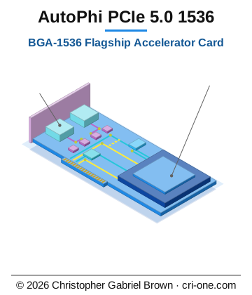
Asset valuation: $7,000,000,000. Project: 44 — AutoPhi PCIe 5.0 1536 Document ID: APV-1536-RENDER-SPEC-001 · Rev: 2 (2026-08-13) Geometry source: blueprints/boards/01-qsfp28-optical/autophi-pcie5-qsfp28-optical-1536-FILLED-sesimport.kicadpcb
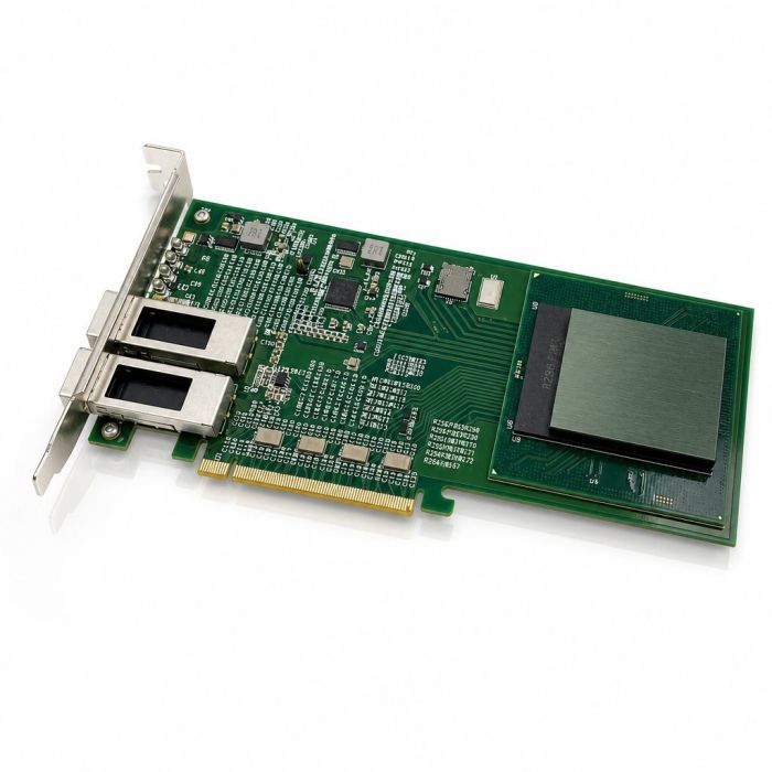
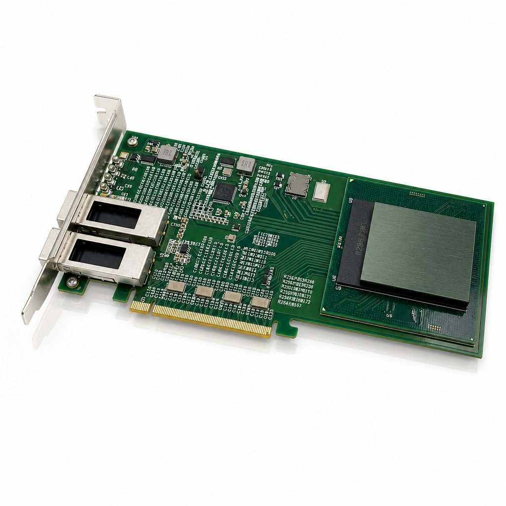
A chip should have somewhere to live. The AutoPhi PCIe 5.0 1536 is that place: a twelve-layer PCI Express Gen 5 add-in card, 256.625 by 111.95 millimetres, drawn as the carrier for the AutoPhi BGA-1536 package. The 1,536-ball part sits as U16 and takes the right-hand third of the board; the left two thirds carry the retimer chain, DDR3 memory, sideband management and a QSFP28 optical front end. Earlier tier boards in this family hold 46 placeholder parts and no main silicon; this one holds 525 real components and the BGA itself.
Every figure here was read from the working KiCad file and checked against KiCad's own export statistics. The card is built on Megtron 6 low-loss laminate with controlled impedance on PCIe, the QSFP28 SerDes and the DDR3 byte lanes. Placement and outline are complete and routing is about seventy percent done - 8,388 track segments, 1,997 vias, 37 copper zones - with the open items listed plainly as engineering state.
This is not a fabrication release. It is a complete engineering data package for the datacenter operator or accelerator buyer who wants the real board: KiCad PCB and schematics, netlists, the flat BOM, the Specctra routing pair, the pinmap for all 1,536 balls, and the 33-script Python pipeline that forks the Texas Instruments TIDA-00423 reference into 34 I/O variants, on an AES-256-encrypted Blu-ray. The design is patent-pending, by Christopher Gabriel Brown, sole inventor. The buyer walks away with the deliverables and the media; the IP, the BGA-1536 package program and the routing pipeline stay with him.
Description
AutoPhi PCIe 5.0 1536 — BGA-1536 Flagship Accelerator Card (SKU 2074)
Project 44 — AutoPhi PCIe 5.0 1536. Document ID APV-1536-RENDER-SPEC-001 , revision 2 (dated 2026-08-13). This is the flagship, fully-populated variant of the AutoPhi PCIe 5.0 line: a 12-layer, HDI-class, 256.625 × 111.95 mm PCI Express Gen 5 add-in card built as the physical carrier for the AutoPhi BGA-1536 hero package (U16, 95 × 90 mm on 2.0 mm pitch). Where the earlier project 35 tier boards carry 46 placeholder parts, no main silicon, and outlines that even kicad-cli cannot resolve, this board carries 525 real components and the BGA-1536 itself . Every geometric figure in this listing was read directly from the working KiCad artefact autophi-pcie5-qsfp28-optical-1536-FILLED-sesimport.kicad_pcb and independently confirmed against kicad-cli 10.0.5 pcb export stats . Nothing here is inferred from a marketing parameter.
Inventor and rights. This card, its 12-layer Megtron 6 stackup, the 1536-ball BGA package it carries, the 34-variant fork of the Texas Instruments TIDA-00423 reference from which its core routing derives, and the surrounding auto-routing / auto-placement / DRC pipeline (approximately 14,000 lines of Python across 33 scripts) were designed and reduced to practice by Christopher Gabriel Brown , sole inventor. The design is patent-pending. All associated schematics, board files, netlists, blueprints, RAG (retrieval-augmented generation) rule bases, and Python pipeline sources are the trade secret and copyright of Christopher Gabriel Brown. Purchase of this listing conveys the physical deliverables and delivery media described in “What Is in the Package” only; it does not convey any implied licence to the underlying IP, to the BGA-1536 die/package program, or to the automated routing pipeline.
Overview
The AutoPhi PCIe 5.0 1536 is the top-of-line member of the AutoPhi PCIe 5.0 family. It shares its outline, its bracket-mount geometry, and its I/O philosophy with the 34 variant boards that were forked from Texas Instruments TIDA-00423 (a PCIe Gen 3 reference design using DS80PCI810 retimers), but it departs from those variants in one decisive respect: it hosts the 1536-ball AutoPhi BGA as U16, and it is placed, escaped, and routed for that package. The BGA-1536 dominates the right-hand third of the card; the left two thirds carry the retimer chain, the DDR3 sub-system, the sideband management interface, and the QSFP28 optical front end.
The card is a full-height add-in card in outline (256.625 mm long, 111.95 mm tall body plus 12.72 mm card-edge tab), fabricated on Megtron 6 low-loss laminate for PCIe Gen 5 (32 GT/s) signal integrity, finished in ENIG for BGA planarity, and built to a 12-copper-layer, symmetric stackup with two dedicated ground reference planes flanking the PCIe high-speed differential pairs. Controlled impedance is targeted at 85 Ω differential on PCIe, 100 Ω differential on QSFP28 SerDes, 40 Ω single-ended on the DDR3 byte lanes, and 50 Ω single-ended generic. The routing state is measured at 8388 track segments, 1997 vias (1753 through, 222 micro, 22 blind), and 37 copper zones ; 128 items remain unconnected and 298 DRC errors remain open, as engineering artefacts rather than as rendered defects (see § “Routing State and Engineering Status”).
The card ships not as a bare-board fabrication release — the design record does not authorise fabrication release — but as a complete engineering data package : the working KiCad PCB and project files, the hierarchical KiCad schematic set, the extracted netlists (KiCad native, XML, and EasyEDA-compatible), the flat BOM (CSV), the Specctra DSN/SES routing pair, the design-rule and stackup specifications, the pinmap for the 1536-ball BGA, the entire 33-script Python pipeline that fork-and-routes the TIDA-00423 into any of the 34 I/O variants, the RAG rule bases that supply net-class widths and clearances, and the render specification against which the marketing imagery was produced. The delivery medium is AES-256-encrypted Blu-ray , described at the end of this listing.
Design Provenance and Position in the Portfolio
Best-3D-model file autophi-pcie5-qsfp28-optical-1536-FILLED-sesimport-RICHER-MODELS.kicad_pcb
KiCad toolchain KiCad 10.0.5 ( kicad-cli 10.0.5 pcb export stats )
Render engine Blender 5.2, Cycles CPU (EEVEE blocked by absent OpenGL framebuffer on the build host)
Inventor of record Christopher Gabriel Brown
Design status Patent pending; engineering complete on placement and outline, routing ~70% complete
The outline is drawn as one properly closed loop of 24 straight segments and 4 arcs — not a bounding rectangle — and it is identical to the coordinate for coordinate in all seven main board variants of the AutoPhi PCIe 5.0 family. Only _fixed.kicad_pcb differs (257.197 × 110.270 mm) and it is not the working file.
Board thickness 1.600 mm nominal (1.640 mm calculated with 2 oz on power planes; 1.570 mm with 1 oz throughout) Stackup
Card-edge finger run X 65.101…149.376: 11.20 mm contacts, 1.862 mm key notch, then 71.213 mm contacts Edge.Cuts
Arcs (4, approx. 180°) r 1.850 and r 1.378 as notch ends; r 1.378 and r 2.385 at the right-hand retention step Edge.Cuts
Body step (lower left) X 35.076…53.426, 8.20 mm deep Edge.Cuts
Coordinate origin Outline top-left corner; KiCad absolute (20.0262, 43.9822) Board-relative convention
Standards note. 256.625 mm is not a standard PCIe length — PCIe half-length is 167.65 mm, full-length 312.00 mm — and 111.95 mm is 0.80 mm over the 111.15 mm full-height figure. The loop is closed and manufacturable, so this is deliberate drawn geometry rather than a leftover default, but the design record does not disclose why it departs from the standard. Purchasers should not describe the card as “full-height full-length”; the geometry does not support the phrase.
Twelve-Layer Stackup
The stackup as configured in autophi-pcie5-qsfp28-optical-1536.kicad_pcb . Two representations of copper weight coexist in the record: an even 0.5 oz on all inner layers (JLCPCB target), and a heavier 1 oz signal / 2 oz power split (Advanced Circuits target). Both are included below and the actual delivered value depends on which fab is selected at production time. The physical layer count and role of every layer are identical across both.
Symmetric stackup is required for BGA-1536 reflow flatness. Total finished thickness is 1.6 mm nominal.
Standard FR-4 exhibits Df ≈ 0.02 at 10 GHz — roughly ten times the loss of Megtron 6 — which becomes prohibitive for PCIe 5.0 (32 GT/s) trace lengths beyond a few inches. Megtron 6 is the de-facto standard for PCIe 4.0/5.0 server hardware. Comparable substitutes accepted by the design (Df ≤ 0.005 at 10 GHz, Dk 3.6–3.8) are Isola I-Tera MT40 , Rogers RO4830 / RO4835 , and Nelco N4000-13EPSI .
KiCad's authoritative component count is 525 : 373 on the front, 152 on the back . Front component density is 22.41% ; back is 1.57% . This is a densely populated card, and the contrast with the project 35 tier boards' 46 parts is the whole point. The file holds 548 (footprint blocks and the extract_pcb_placement.py utility resolves 523 with positions; KiCad's 525 is the authoritative count.
U16 dominates the right-hand third. At 95 × 90 mm centred on (203.50, 49.17) the BGA-1536 spans X 156…251 and Y 4.2…94.2, leaving roughly 5 mm to the right board edge and 4 mm to the top edge . On a 256 × 112 mm card it occupies about one third of the length and nearly the full height. This is the opposite of the project 35 tier boards, where the largest part is a 7 × 7 mm QFN. Any depiction of this card that fails to make U16 the visual subject is factually wrong.
The board is routed, substantially but not completely , in the -sesimport variants. Measured against the project's own design rules (not KiCad's stock defaults — see the “DRC Trap” note below):
This is HDI-class work , consistent with the project's declared minimums: 0.0762 mm track, 0.2032 mm via, 0.127 mm hole. The 298 open errors are dominated by 159 clearance violations (netclass Power wants 0.150 mm, actual 0.1331 mm — a near-miss, not a collision), 82 front solder-mask bridges , 38 starved thermal reliefs , and 12 shorting items . The shorts are the only category that is unambiguously serious and must be resolved before any fabrication release.
DRC trap. kicad-cli pcb drc reads design rules from the sibling .kicad_pro . The -RICHER and -RICHER-MODELS variants have no project file, so KiCad silently falls back to stock defaults — min track 0.2 mm, via 0.5 mm, hole 0.3 mm, annular 0.1 mm. This board is HDI: 0.125 mm tracks, 0.36 mm vias, 0.2032 mm drills. Run against the defaults it reports ~1200 phantom track_width / via_diameter / annular_width / drill_out_of_range errors that are purely an artefact of the missing file. Always DRC -FILLED-sesimport , which has its .kicad_pro .
pcie_diff 0 PCIE_TX* , PCIE_RX* 0.127 mm (5 mil) 0.127 mm 0.127 mm 0.127 mm 1.27 mm (50 mil)
Guard-band to other pairs ( guard_mm ) is 0.508 mm (20 mil, 5W-style) for both pcie_diff and refclk . Maximum via pair counts are 4 (TX) / 2 (RX) for pcie_diff ; 2 / 2 for refclk . Route order follows lower priority = routed earlier: high-speed differentials and reference clock first, then DDR, then control, then power — a citation-based ordering that lives in autophi_engine/rag/routing.py .
Layer-specific (pseudo-blind) 0.20 mm 0.45 mm KiCad (layers "F.Cu" "In2.Cu") — through-drill but electrically restricted
GND stitching 0.20 mm 0.45 mm 5.0 mm grid across board
The design specifically avoids blind/buried vias (outside JLCPCB standard process) and uses layer-specific through-vias where a restricted electrical connection is required. Maximum hole aspect ratio 10:1 (1.6 mm board → 0.16 mm min drill; 0.20 mm is used).
Placement Standard — BGA and Left-Edge I/O Anchoring
The design uses a reusable anchor standard for the primary BGA and left-edge IN/OUT connectors, so the same cluster can be re-used across the 34 I/O variants without re-authoring geometry:
Connector locking rule: J2 and J3 keep fixed deltas from U1; when the BGA moves, both connectors translate by the same vector, preserving IN/OUT spacing across variants. This is enforced by blueprints/apply_bga_io_standard.py .
The Auto-Routing / Auto-Placement Pipeline
This board is not a hand-drawn artefact. It is one deterministic output of a 33-script, approximately 14,000-line Python pipeline that transforms the Texas Instruments TIDA-00423 reference design into all 34 AutoPhi PCIe 5.0 product variants. A one-command driver, python blueprints/build_all.py , runs the five pipeline stages: fork → place → route → DRC → export. The complete pipeline is included on the delivery media.
auto_route.py 1,749 A* maze router: grid routing, differential-pair, row-to-layer fanout, DRC halos
The router ( auto_route.py ) is a grid A* maze router that writes the .kicad_pcb file in place. After each successful write it invokes kicad-cli pcb drc when the CLI is on PATH or at a typical Windows install location (override with KICAD_CLI ). Notable behaviours:
- Target-first chaining. Route connector or retimer before the BGA using R.NET_PAD_ORDER["target_first_refs"] , default U1 . Override with --target-first-refs REFS .
- Global-then-detailed A*. R.GLOBAL_ROUTE runs a coarse tile BFS on the start layer, builds an inflated fine-cell corridor, then runs detailed A* inside it; falls back to full-grid A* if that fails. Disable with --no-global-route .
- Backoff on failure. Second-pass retry follows R.A_STAR["backoff_if_fail"] .
- Cached / incremental routing. Route cache under blueprints/route_cache/ with run_metrics.jsonl for progress tracking.
- Row-to-layer BGA fanout. BGA rows map deterministically to escape layers; see ROUTING_TECHNIQUE_ROW_LAYER_FANOUT.md .
- Congestion-heatmap analysis. DDR address hotspots identified before routing; see ROUTING_TECHNIQUE_CONGESTION_HEATMAP.md .
Renderer
render_board_svg.py is a pure-Python SVG renderer that bypasses kicad-cli (which cannot open the forked .kicad_pcb files — the fork header claims version 20260206 but uses older tstamp s-expressions). The renderer draws front parts in gold pads ( #e7b74d ) with white courtyard outlines, back parts in cyan pads ( #5dc1d9 ) with muted cyan outlines, and every SMD gets a bounding-box outline so collisions are visible at a glance.
Schematic and Netlist Architecture
The active schematic is a hierarchical KiCad tree (generator 2.1) with an index sheet at blueprints/boards/01-qsfp28-optical/autophi-pcie5-qsfp28-optical.kicad_sch and subsheets under autophi-v19-variant-01-qsfp28-optical_sheets/ . Sheets are:
- 01_central.kicad_sch — the BGA-1536 central processor (U16), with hierarchical labels bound to the 1536-ball pinmap and DDR3 / QSFP28 / management interfaces.
- 02_pcie_retimers.kicad_sch — U3, U6, U17, U21 (four PCIe retimers, one per group of four lanes) using the AutoPhi symbol library, wired to PET*/PER* label groups and to +3.3V , SMCLK/SMDAT , and DS_READ_EN / DS_ALL_DONE / DS_EN_SMB / DS_PWDN_N control lines.
- 03_pcie_x16_edge_connector.kicad_sch — J5 (PCIe ×16 gold-finger card edge), all PETp0..PETp15 , PETn0..PETn15 , PERp0..PERp15 , PERn0..PERn15 plus REFCLK± , PERST# , WAKE# , CLKREQ# , SMCLK , SMDAT , PRSNT1# , PRSNT2# , TRST# .
- 04_power_tree.kicad_sch and 04b_ddr3.kicad_sch — DDR3 sub-system (four FBGA-96 DDR3 SDRAM x16 devices in the 1536 configuration: U4, U9, U19, U31), shared address/command bus, per-chip data lanes DDR_DQ0 … DDR_DQ63 , per-chip strobes, VREFCA and per-chip VREFDQ, one 240 Ω ZQ resistor per chip; TPS62133-class buck to 1V5, TPS51200-class VTT to VTT_DDR/VREFCA, and 40 Ω VTT termination resistors at bus end.
The netlist is available in four representations: KiCad native .net , KiCad .xml , EasyEDA-compatible .json and .net , and a flat .csv BOM. The TI TIDA-00423 complete netlist is included as both structured JSON and rendered Markdown for provenance.
Bill of Materials — Sourcing
Sourcing policy: the AutoPhi BGA-1536 die and package program (U16) is the only custom / non-catalogue silicon on the card. Every other line item is chosen from commercial-vendor catalogues (Texas Instruments where the reference design calls for it — e.g. DS80PCI810 retimers — plus DRAM, connectors, passives, PMICs, etc. from their normal supply chains and MPNs).
Role Refs Part / class Notes
Main SoC / accelerator U16 (1536 variant); U1 in reference-family shared symbol AutoPhi BGA-1536 Only non-vendor-catalogue part. Christopher Gabriel Brown's die and package program.
PCIe retimers U2–U5, U8 (family); U3, U6, U17, U21 in the 1536 schematic instance TI DS80PCI810 (QFN-64) Real, orderable bridge between edge and MAC, per TIDA-00423.
DRAM U4, U9, U19, U31 (1536 configuration) DDR3 SDRAM, FBGA-96, ×16 Speed grade and density per board inventory and timing budget.
Host edge J5 PCIe ×16 gold-finger card edge, 1 mm pitch PCI-SIG CEM 5.0 mechanical + electrical.
Optical I/O J6, J8 Amphenol U95T151100A QSFP28 cages Both rotated −90°; the variant-01 QSFP28 optical bracket.
Storage J4 Hirose DM3AT-SF-PEJM5 microSD socket Rotated 180°. Note: not an optical cage, despite this board living under 01-qsfp28-optical/ .
Mechanical MH1, MH2 (plus MH3–MH6 in family) M3 mounting Must be on real GND net to avoid unconnected- DRC and to close return-current paths.
Regulators U_1V5, U_VTT1 DFN-package point-of-load regulators Named power rails.
ESD arrays 2× TPD4E004 4-line ESD protection On sideband and slow-speed lines.
Bulk decoupling 4× Radial electrolytic, 10.0 mm diameter Only tall through-hole parts on the card.
NTC thermistors RT-series (in family variants) Distributed inter-chip and under-BGA Thermal telemetry.
- Open PCIe ×16 slot (electrical and mechanical; full-height matches the bracket).
- Continuous +12 V, +3.3 V, and +3.3 V AUX headroom per the board's power map.
- Case airflow or GPU-style shroud if TDP is non-trivial (the card ships bare; no heatsink is included — see § “What the Record Does Not Contain”).
- OS and driver path: for standard PCIe class devices plan a signed or in-box driver; for custom-class devices plan an attestation story.
Tomorrow (rack server / data-centre host)
- Same electrical lane budget, or deliberate bifurcation / retimer path if the link is split.
- Front-to-rear airflow, inlet-temperature class, N+1 fan policy where required.
- BMC / inventory: FRU EEPROM or SMBus plan for chassis-blind discovery.
- Security: firmware-update channel; secure-boot interaction if there is an option ROM or management endpoint.
- Server-grade bracket / EMI finger stock as needed by the variant.
- Vibration and shock notes for heavy heat sinks or optical modules.
JLCPCB (primary) 6–20 layer, POFV free on 6L+, controlled impedance free on multilayer Production
Ballpark is a 5-piece prototype of roughly 6 × 4 inch (152 × 102 mm) area; the 1536 board's 256.625 × 111.95 mm outline is larger and cost scales proportionally. Lead time: 2–3 weeks standard, 7–10 days rush (1.5×–2× cost).
What the Design Record Does Not Contain
The following are explicitly absent from the design record and are called out here so the purchaser is not misled:
- Routing is ~70% complete, not finished. 128 unconnected items and 298 DRC errors remain, including 12 shorting items. The shorts and the remaining connectivity must be resolved before the card is presented as a released product. Everything needed to depict the card exists.
- No solder mask colour is recorded. Matte green is assumed throughout the portfolio. If the intended mask is black, blue, or matte white, every existing render is wrong.
- No surface finish is recorded for the card-edge fingers ; ENIG gold is assumed.
- No silkscreen colour beyond the assumed white.
- Three 3D models carried stale absolute paths to C:/Users/crione/Chris/special/ , a directory from another machine — including U16's own interposer and die models and the PCIe bracket. All three files exist under D:/special/ at identical relative paths. Until the references are repointed, any 3D export of this board silently omits the hero package.
- No enclosure, heatsink, or thermal solution. A 95 × 90 mm BGA of this class would not ship bare; nothing in the record describes a cooling solution.
- No bracket geometry beyond the STEP model and its presence.
- Board mass and stack material are not recorded.
What Is in the Package
This listing delivers the complete engineering data package for the AutoPhi PCIe 5.0 1536 board on a single AES-256-encrypted Blu-ray, containing:
- Working KiCad PCB file — autophi-pcie5-qsfp28-optical-1536-FILLED-sesimport.kicad_pcb (525 components; 8388 routed track segments; 1997 vias; 37 copper zones).
- Best-3D-model KiCad PCB file — autophi-pcie5-qsfp28-optical-1536-FILLED-sesimport-RICHER-MODELS.kicad_pcb (identical routing; richer STEP models for 3D export).
- KiCad project file autophi-pcie5-qsfp28-optical-1536.kicad_pro carrying the design rules the DRC must be evaluated against.
- Hierarchical KiCad schematic set (index sheet plus 01_central , 02_pcie_retimers , 03_pcie_x16_edge_connector , 04_power_tree , 04b_ddr3 subsheets), generator 2.1, with the BGA-1536 override applied.
- Extracted netlists: KiCad native .net , KiCad .xml , EasyEDA-compatible .json / .net , and the flat CSV BOM (both v3 reference and this-board extract, plus bom_vs_v3_report.txt drift analysis).
- Specctra routing pair ( .dsn and .ses ) for Freerouting interoperability.
- Pinmap for the 1536-ball AutoPhi BGA ( AUTOPHI_BGA1536_pinmap_working.csv ) and the KiCad footprint AutoPhi:BGA-1536_95x90mm_P2.0mm .
- The complete auto-routing / auto-placement / DRC pipeline: 33 Python scripts, approximately 14,000 lines of code, with build_all.py master orchestrator.
- RAG rule bases ( autophi_engine/rag/routing.py , components.py , and companion tables) that supply net-class widths, clearances, via limits, fabrication constraints, and JLCPCB tables.
- Complete documentation set: RENDER_SPECIFICATION.md , MANUFACTURING.md , STACKUP_SPEC.md , RULES_DDR_PCIE.md , VARIANTS.md , BGA_IO_STANDARD.md , SCHEMATIC_PROCESS.md , SCHEMATIC_CONNECTION_METHOD.md , KICAD_PLUGIN.md , SOURCE_OF_TRUTH.md , HANDOFF.md , ROUTING_PROCESS.md , ROUTING_RECURRING_PROCESS.md , ROUTING_DRC_MECHANISM.md , ROUTING_TECHNIQUE_DIFF_PAIR.md , ROUTING_TECHNIQUE_ROW_LAYER_FANOUT.md , ROUTING_TECHNIQUE_CACHED_INCREMENTAL.md , ROUTING_TECHNIQUE_TARGET_FIRST.md , ROUTING_TECHNIQUE_CONGESTION_HEATMAP.md , ROUTING_CHECKPOINT_v7.md , INTEGRATION_parts_today_tomorrow.md , the TI_TIDA00423_COMPLETE_NETLIST pair (JSON + Markdown), and the COOKBOOK_FINAL.md assembly recipe.
- Wiring artefacts and traceability: DDR3 pin assignment, DDR3 power-tree additions, IC-to-FPGA connection batches 1–4, floorplan proposal for J5 / U16, POWER_AC_BYPASS_SPEC, STACKUP_SPEC, and the ERC report series ( erc_baseline_256 , erc_after_sheet01 … erc_after_all , erc_1536 ).
- Snapshots of the build at two engineering checkpoints ( snapshots/r4_before_powergnd/ and snapshots/r10_schematic_pipeline/ ), each with its own frozen scripts, HANDOFF, ROUTING_PROCESS, and (for r10) full autophi_bom_v3.csv , autophi_netlist_v3.net , autophi_netlist_v3.xml , and MANUFACTURING.md .
- KiCad auxiliary artefacts: interactive placement editor HTML, schematic viewer HTML, batch route driver batch_route_03_34.sh , Allegro import script import_to_allegro.scr , and Allegro SKILL generator.
- Cross-format converters ( easyeda_to_kicad.py , kicad_to_dsn.py , ses_to_kicad.py , kicad_to_eagle.py ).
- Render specification (this document's parent, RENDER_SPECIFICATION.md revision 2) and the reference imagery produced against it (top-down and three-quarter views).
- A signed statement of provenance identifying Christopher Gabriel Brown as the sole inventor of record.
Not included: physical fabricated PCB, physical BGA-1536 silicon, any physical hardware whatsoever, any right to fabricate at scale, any right to redistribute the pipeline sources, any right to re-brand the AutoPhi silicon program.
Delivery
Delivered on a single-layer or dual-layer Blu-ray disc (25 GB or 50 GB, sized to the archive), written as a UDF 2.60 volume, with the entire payload sealed inside an AES-256-CBC encrypted archive . The decryption passphrase is transmitted separately to the purchaser's verified e-mail address of record on cri-one.com/store after the order clears, and never appears on the disc, its case, or its printed label. Discs are hand-labelled with SKU 2074 and the project key 44-autophi-pcie5-1536 , packaged in a rigid case, and shipped by tracked courier. On receipt, verify the disc's SHA-256 against the value provided in the shipping e-mail before decrypting; if the hashes disagree, do not proceed — contact the store and return the disc for replacement. The passphrase, once used, should be stored offline; loss of the passphrase means loss of access to the archive, and neither the store nor the inventor retains a copy.
© 2026 Christopher Gabriel Brown. All rights reserved.
Photo
Footnotes
- Product number 8493.
- Family: autophi pcie cards.
- Purchase: When you buy, you buy the use of that blueprint only.