
23-zetta-flops
Asset valuation: $14,000,000,000. Master index of all projects: PROJECTSINDEX. Last edited: 2026-05-02 Status: Multi-project bundle targeting zetta-FLOPS-class compute throughput Maturity (per PACKAGEARCHITECTURE.md): L4 (Tape-out / Mass-Manufacturable) — bundles foundry-ready AutoPhi content
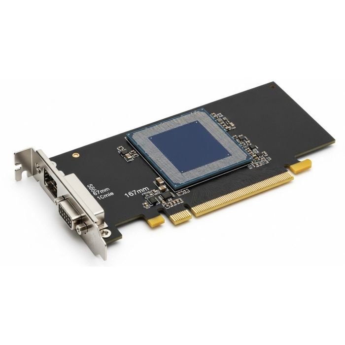
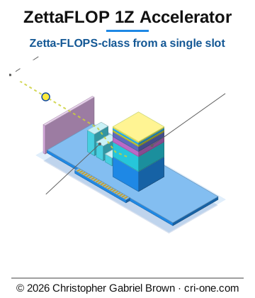
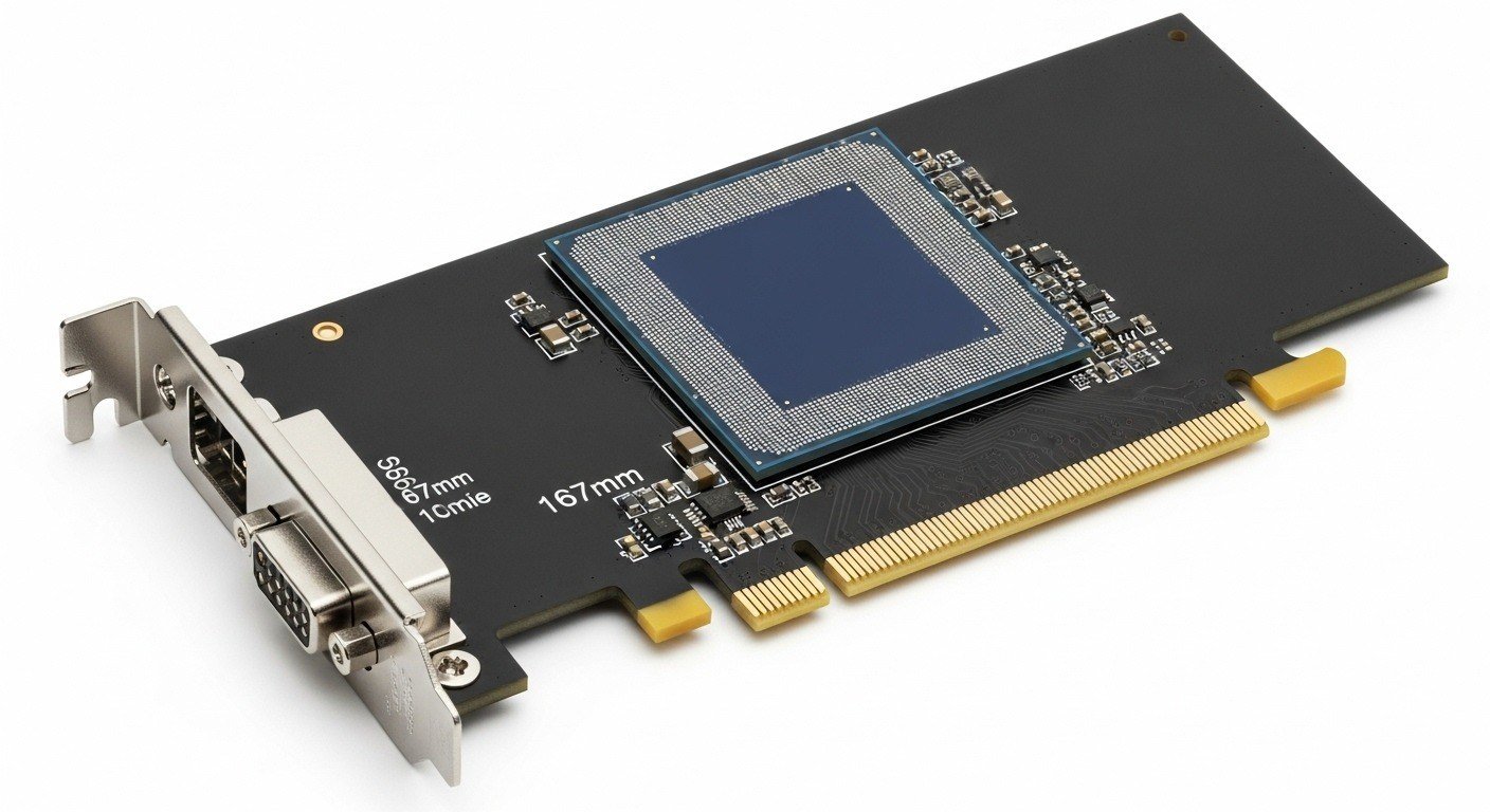
Imagine a single PCIe card that drops into one server slot and brings zetta-FLOPS-class throughput with it. That is the ZettaFLOP 1Z Accelerator. It is original silicon, not RISC-V, ARM or x86. Its Light CPU does arithmetic in colour - red light adds, blue subtracts, green multiplies, yellow divides - and a single-photon Light Trigger starts each operation, with micro mirrors steering the light. Beside it runs a 64-qubit Quantum CPU with sixteen instructions of its own, holding fidelity above 95 percent and up to 99.95 percent with Light Trigger assist. The whole thing is stacked 500 layers tall on a 36 mm square die, five millimetres from bottom to top: compute first, then memory and nanophotonic interconnect, vertical threading, quantum error correction, quantum battery, electromagnetic cooling, and finally I/O and power.
Five configurations ship on the same design: REV-1 at 1.75 ZFLOPS, REV-4 at 2.50 ZFLOPS, the REV-5 "Ultimate" at 3.50 ZFLOPS with 1.1 PB of memory at 78 PB/s, a MicroSDXC card at 512 GFLOPS, and a five-chip Set of Five. The package bundles four projects - AutoPhi Modern, AutoPhi Future, the Communications Satellite I/O subsystem and the Day-One Fabrication toolchain - into one foundry-ready deliverable, with six synthesizable Verilog modules and all 579 verification tests passing. It is for the datacenter operator who wants a great deal of compute in very little rack, and the engineering buyer who wants to read it in RTL first. You walk away with the complete foundry handoff; the patents and the architecture stay with the inventor.
Description
Patents: USPTO 18/370,908, 19/540,453, 29/839,062 (Light Trigger), 3561 2876 (Cold Light Micro Chip), 1026 (LED Recycle), 1096/1097/1098 (Electromagnetic Cooling)
Status: L4 Tape-out — 579/579 verification tests passing across 47 layers, foundry handoff package complete
Overview
The ZettaFLOP 1Z Accelerator is a PCIe 5.0 x16 compute card delivering zetta-FLOPS-class throughput from a single slot. The package bundles four sub-projects into one foundry-ready deliverable: AutoPhi Modern (Project 02 — 12 generations, 120 chips, APM01–APM12), AutoPhi Future (Project 18 — voxel-as-cell architecture with photon chromosomes), Communications Satellite (Project 19 — high-bandwidth I/O subsystem), and Day-One Fabrication (Project 21 — RTL-to-mask toolchain).
This is original silicon — not RISC-V, ARM, or x86. The architecture uses Color Mathematics, where colored light signals encode arithmetic operations. A single-photon Light Trigger initiates computation through digital micro mirrors and staircase mirrors for optical routing and temporal delay processing.
The Light CPU core runs a 6-state pipeline: IDLE → TRIGGER → COLOR_DECODE → OPERATION → MIRROR_REFLECT → COMPLETE. Internal registers include an 8-bit light accumulator, 16-bit mirror delay counter (initialized at 100 cycles), and a 3-bit mirror angle routing output derived from the computation result.
64-Qubit Quantum CPU — 16 Custom Instructions
The quantum processor runs a 10-state machine (IDLE, DECODE, SECURE_INIT, QUANTUM_OP, MEASURE, ERROR_CORRECT, SANITARY_CHECK, SECURE_COMPUTE, VERIFY, COMPLETE) with configurable qubit count (64 default, supports 128+) and security levels 1–5. Fidelity: 95%+ maintainable, 99.75%–99.95% with Light Trigger assist.
Security Domain (4 instructions):
- QINST_SECURE_INIT (0x01) — Initialize secure quantum state
- QINST_SECURE_ERASE (0x05) — Cryptographic state erasure
- QINST_SECURE_TRANSFER (0x09) — Encrypted quantum data transfer
- QINST_SECURE_COMPUTE (0x0E) — XOR with 4 encryption keys, tamper detection via hash comparison
Performance Domain (5 instructions):
- QINST_QUANTUM_ADD (0x02) — Quantum addition via XOR
- QINST_QUANTUM_MUL (0x03) — Quantum multiplication via AND with entanglement
- QINST_QUANTUM_SEARCH (0x0A) — Grover-style quantum search
- QINST_QUANTUM_FACTOR (0x0B) — Quantum factorization
- QINST_ENTANGLE (0x0C) — Qubit entanglement
Sanitary Domain (4 instructions):
- QINST_SANITARY_CHECK (0x08) — XOR-based integrity hash validation
- QINST_ERROR_CORRECT (0x07) — Error correction (fidelity +5, error rate −2/−5)
- QINST_QUANTUM_MEASURE (0x04) — Measurement collapse to |0⟩
- QINST_QUANTUM_VERIFY (0x0F) — State verification
Advanced Domain (3 instructions):
- QINST_QUANTUM_COPY (0x06) — Quantum state duplication
- QINST_DISENTANGLE (0x0D) — Qubit disentanglement
- QINST_QUANTUM_VERIFY (0x0F) — Advanced state verification
- ZETTAFLOP_1Z_ACCELERATOR_top — Top-level wrapper. Parameters: DESIGN_ID, DESIGN_VERSION, QUBITS=64, CLASSICAL_BITS=32, SECURITY_LEVEL=3, ACCELERATOR_TYPE=0, STACK_LAYERS=500, MAX_HEIGHT_UM=5000, LAYER_PITCH_UM=10. Contains all I/O declarations for CPU, PCIe 5.0 x16, all nine technology interfaces, MicroSDXC, and performance counters.
- autophi_scale_accelerator_integration (371 lines) — CPU-Accelerator bridge. 512-bit data packing/unpacking, memory request/grant handshaking, accelerator instruction injection. Data packing format: quantum_result[31:0], color_result[39:32], operation_mode[41:40], quantum_state[105:42], total_operations[137:106], with 382-bit padding.
- autophi_hybrid_cpu_top (158 lines) — Hybrid CPU integration. Instantiates both Light and Quantum CPUs. Coordinates operations, tracks light_ops_count and quantum_ops_count, generates combined completion signal, verifies security (secure_mode AND NOT tamper_detected), performance (ops count > 0), and sanitary status (sanitary_clean AND fidelity > 90%).
- autophi_light_cpu_core (177 lines) — The Color Mathematics engine described above.
- autophi_quantum_cpu_core (297 lines) — The 64-qubit processor described above. Internal registers: qubit_states array, entanglement_map, coherence_time (starts at 100, counts down), error_correction_level, security_hash, integrity_hash, 4 encryption keys (8-bit each), corruption_detector.
- autophi_accelerator_interface_adapter (207 lines) — Multi-protocol adapter. 5-state machine: IDLE, ADAPT_PCIE, ADAPT_SDXC, ADAPT_SET_OF_FIVE, WAIT_COMPLETE. Formats output for PCIe (512-bit for REV-1/4/5), SDXC (4-bit for MicroSDXC), or multi-chip (5 × 128-bit for Set of Five).
- Base threads: 268,435,456
- Stack layers: 62,515
- Clock range: 4 GHz (min) / 8 GHz (standard) / 16 GHz (max)
- Minimum FLOPS = 268,435,456 × 4 GHz × 1 op/cycle = 1.074 ExaFLOPS
- With Light Trigger boost (2x): 2.148 ExaFLOPS
- With mirror efficiency (40.82%): 877 PetaFLOPS standalone baseline
Scale-64 Maximum + REV-5:
- Base threads: 268,541,696 at 16 GHz = 4.297 ExaFLOPS
- With Light Trigger (2x) + GREEN Color Math (2x): 8.594 ExaFLOPS
- Combined with REV-5: 3.509 ZettaFLOPS
Comparison: Scale-1 CPU alone = 877x faster than NVIDIA H100. Scale-64 + REV-5 = 3,508,594x faster.
1. LED Power Recycling (Patent 1026) — 90% photon capture efficiency, 42% net power reduction. 16-bit photon level sensing. RTL signals: ambient_light_level[15:0] , led_emission_level[15:0] , energy_harvested[31:0] , power_efficiency[15:0] (9000 = 90%).
2. Vertical Threading — 12,000 TSVs/mm², 125 TB/s inter-layer bandwidth. 18 data layers, 64-bit per layer. RTL: layer_data_in[63:0][17:0] , layer_data_out[63:0][17:0] .
3. Chiplet Stacking — 500 layers, 5 mm max height, ~10 μm pitch, 18 chiplets per stack, 28 stacks maximum. TSV bonding with nanophotonic waveguide alignment.
4. Nanophotonic Data Flow — 1,400 TB/s total bandwidth across 2,800 optical channels at 0.5 TB/s each. 256-bit per channel, 3 WDM wavelength control registers. RTL: photonic_data_in[255:0][2799:0] , photonic_data_out[255:0][2799:0] .
5. Quantum Error Correction — 99.998% accuracy, 1,400 logical qubits, 1 MHz error correction cycle, 32-bit per qubit data width. RTL: quantum_data_in[31:0][1399:0] , quantum_fidelity_accel[31:0] , coherence_time_status[31:0] .
6. Electromagnetic Cooling (Patents 1096/1097/1098) — 97% efficiency, 32 independent thermal zones, zero moving parts, near-zero power consumption. Target operating: 45–65°C. Max junction: 105°C. RTL: temperature_sensors[15:0][31:0] , cooling_control[15:0][31:0] .
7. Quantum Battery Layers — 20 layers, 1,500 Wh capacity, 75 MW burst power, integrated within the 5 mm stack. RTL: battery_charge_level[15:0] , battery_capacity[31:0] , discharge_rate[31:0] .
8. Quantum-Classical Hybrid Interface — Single-cycle handoff latency. 64-bit quantum data, 64-bit classical data, 64-bit result. RTL: hybrid_quantum_data[63:0] , hybrid_classical_data[63:0] , hybrid_result[63:0] , hybrid_ready .
9. Neuromorphic AI Engine — Near-zero idle power, event-driven activation. 32-bit spike interface. RTL: neuromorphic_spike_in[31:0] , neuromorphic_spike_out[31:0] , neuromorphic_ready .
PCIe 5.0 x16 Interface
- 16 differential pairs (TX + RX), 32 GT/s per lane, 512 GT/s total (64 GB/s)
- 100 MHz differential reference clock ( pcie_refclk_p , pcie_refclk_n )
- PERST# active-low reset
- 32-bit configuration space with 12-bit address
- Power: 75 W from slot + 225 W auxiliary (1 × 8-pin + 1 × 6-pin) = 300 W available
- Actual power required: ~140 W after LED power recycling — significant thermal margin
- Core voltage: 0.7–1.0 V (process-dependent), I/O: 1.8 V / 3.3 V
Memory Hierarchy
- 64-bit address bus, 512-bit data bus
- 3 memory types via 2-bit selector: 00=quantum, 01=photonic, 10=neuromorphic
- Photonic memory: 2,800 channels at 0.5 TB/s each
- Quantum memory: 1,400 logical qubits at 32-bit per qubit
- Neuromorphic cache: near-zero idle power, event-driven
- REV-5 maximum: 1.1 PB capacity, 78 PB/s bandwidth
Manufacturing Cost Breakdown (COGS: $91,300/card)
Year-1 list price: $150,000–$250,000 (39%–64% margin). Volume discounts: 10% at 11–50 units, 15% at 51–100, 20% at 101–500. COGS reduces 15%–25% at 10,000+ units/year. Lead time: 8–12 weeks after foundry fabrication. 1-year warranty standard (3-year and 5-year extended available).
EDA Flow
- Synthesis: Yosys — 4 scripts in synthesis/ , producing netlists in Verilog, JSON, and DOT graph formats (7 output files)
- Place & Route: OpenLANE — config.json , config.tcl , config_14nm.tcl , config_7nm.tcl
- Outputs: GDSII layout, SDC timing constraints, DEF placement, LEF abstracts
- SDC Timing: Input delay max 1.5 ns / min 0.3 ns (pcie_refclk domain), output delay max 1.5 ns / min 0.3 ns, false path on pcie_perst_n
- Automation: 4 shell scripts — generate_gdsii.sh , run_all_simulations.sh , run_openlane.sh , run_synthesis.sh
- Verification: 6 testbenches, 1 test vector file, 579/579 tests passed across 47 verification layers (100% pass rate, dated February 27, 2026)
- AutoPhi Modern (Project 02) — 12 generations, 120 chip designs (APM01–APM12), core RTL compute substrate. Includes 5-year plan, valuation summary, and the complete AutoPhi Unit (Project 28).
- AutoPhi Future (Project 18) — Next-generation voxel-as-cell architecture with photon chromosomes and Blu-ray foundry packages. 11 documentation files including deep-dive pitch, miracle calculation, processor power comparison, and seed voxel scaling analysis. 9 HTML pitch files.
- Communications Satellite (Project 19) — High-bandwidth I/O subsystem for the compute fabric.
- Day-One Fabrication (Project 21) — RTL-to-mask toolchain including the AutoPhi Scale accelerator integration module, verification report across all layers, and Python performance verification scripts.
What Is in the Package
- Source folder: 23-zetta-flops
- 137 total files (per MANIFEST.json): 73 documentation, 19 HDL (Verilog), 16 web (HTML), 5 EDA outputs, 4 data, 2 source code, 1 image, 1 layout
- 6 synthesizable Verilog RTL modules (1,200+ lines)
- 4 Yosys synthesis scripts with 7 netlist outputs
- 4 OpenLANE configurations (generic, 14 nm, 7 nm)
- GDSII layout + SDC/DEF/LEF foundry outputs
- 6 testbenches + test vectors
- Package specification: ZETTAFLOP_1Z_ACCELERATOR_package_spec.txt
- 10 architecture documents (including the ones detailed above)
- Complete patent reference file with prior-art analysis (scan completed 2026-05-11)
- CITATION.cff (CFF 1.2.0 format), CHANGELOG.md, hero image SVG
- Four complete sub-projects with their own documentation
How this is delivered
This package ships on a single Blu-ray disc, posted to the delivery address on your order. The archive on the disc is AES-256 encrypted; the passphrase is sent separately, by email, once the disc is despatched — so the disc alone is of no use to anyone who intercepts it.
Discs are despatched by tracked, signed-for post. Allow 5 business days for mastering and verification before despatch.
Photo
Footnotes
- Product number 8471.
- Family: autophi on demand.
- Purchase: When you buy, you buy the use of that blueprint only.