
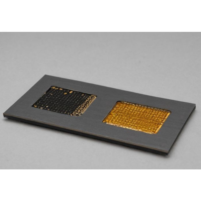
15-smd
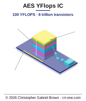
Asset valuation: $600,000,000. Status: L2 (Designed) — packaged design, not yet fabricated Last edited: 2026-05-04 (per ZIP archive timestamp) Inventor: Christopher Gabriel Brown Contact: christopher@cri-one.com ·Email: christopher@cri-one.com
A chip should not have to be flat. Silicon dies stop at about a millimetre of height because heat and cost say so. The Semiconductor Method Discovery package starts from a different substrate, a two-element alloy the inventor calls AES, and the ceiling comes off. On AES a die can stand ten millimetres tall, built up through roughly five hundred and fifty nanolayers organised into thirty-two working layers, and still move its heat through the stack.
The reference part is AES-YFLOPS-100-IC: eight trillion transistors in a 32 by 32 millimetre footprint, 5.8 GHz, 235 watts, one hundred yottaflops peak. On one substrate it carries classical logic, a quantum array of one billion physical qubits, a hundred-billion-neuron neuromorphic engine and thirty thousand nanophotonic channels, with no third-party ICs anywhere in the design, on a half-height, half-length PCIe card. It is designed, not fabricated: complete RTL, layout, constraints, synthesis scripts, DRC, LVS, timing and power reports, a datasheet and foundry handoff documentation, ready for a fab to pick up. A fifty-claim utility patent application is filed and pending at the USPTO.
This is for frontier-compute and national-scale AI buyers, and for the engineering buyers and licensees who want the process itself. The buyer is not paying for a chip; the buyer is paying for a way to make a chip that silicon cannot make. The alloy's element pair, ratios and deposition recipe are trade secrets that stay with the inventor and open only under NDA at the appropriate tier.
Description
Copyright: © 2026 Christopher Gabriel Brown (AutoPhi / CRI-ONE). All rights reserved.
Patents: USPTO 19/449,352 — “Semiconductor Method Discovery” — 50 claims, utility application filed January 14, 2026, pending examination at USPTO Patent Center. Umbrella application US 19/540,453 may also apply (verify before claiming coverage).
Status: L2 (Designed) — foundry-handoff-ready packaged design. Complete RTL, layout (LEF/DEF with GDS placeholder), constraints, synthesis scripts, DRC/LVS/timing/power reports, datasheet, and foundry handoff documentation. Not yet fabricated; no physical chip exists. The archive includes 27 files totalling approximately 62 KB.
Overview
AES-YFLOPS-100-IC is a packaged custom integrated-circuit design for an AES (Advanced Encryption Standard) accelerator with a yottaflops-class throughput envelope, implemented as a nanolayer-stacked quantum-array IC on the inventor’s proprietary AES substrate. The part number is SMD-15-2026-AES-YFLOPS-100 .
The design delivers 100 YFLOPS peak performance (1.0 × 10 26 FLOPS) from 8 trillion transistors packed into a 32 × 32 mm footprint that stands 10 mm tall — roughly ten times the height of any conventional silicon IC. The die is built up through approximately 550 physical nanolayers of AES deposition and interconnect, organised into 32 active functional layers . It runs at 5.8 GHz and draws 235 W TDP , yielding approximately 4.25 × 10 23 FLOPS/W (425 zetta-FLOPS per watt). It ships on a PCIe Half-Height Half-Length (HHHL) card (167.65 × 68.90 mm, PCIe 5.0 x16 with 8 lanes wired in this reference design). The die covers roughly 19% of the card’s length and 46% of its height — it is the dominant object on the board.
The compute role is a complete unit: quantum + classical + photonic + neuromorphic on a single AES substrate. The intended use cases are frontier compute, national-scale AI, and scientific simulation. All IP is custom — no third-party ICs are used anywhere in the design. The buyer is not paying for a chip; the buyer is paying for a way to make a chip that silicon cannot make.
Why AES Makes This Possible
Conventional silicon has hit thermal and economic walls at the high end of AI compute. The largest production silicon AI accelerators sit in the exa-FLOPS range. This part operates in the yotta-FLOPS range — six orders of magnitude beyond — at a fraction of the wall-plug power, because the proprietary AES substrate relaxes every constraint that caps silicon die height at approximately 1 mm.
Property AES Substrate Silicon Advantage
Bandgap Direct 0.8 eV 1.12 eV (indirect) Optimal low-voltage switching window; sub-volt logic with manageable leakage across 550 layers
Electron mobility 12,000 cm²/V·s ~1,500 cm²/V·s 8× silicon — enables 5.8 GHz at 8 trillion transistors and 235 W
Hole mobility 8,000 cm²/V·s ~450 cm²/V·s 17.8× silicon
Thermal conductivity 400 W/m·K ~150 W/m·K 2.7× silicon — through-stack heat dissipation works across 550 nanolayers
Substrate cost ~$5/kg Wafer cost dominant Orders of magnitude cheaper; 10 mm stack is economically feasible
Alchemy Data V2 score 100/100 Partial overlap Top-ranked across all semiconductor mechanism categories out of 2,000 candidates
AES emerged from the Project 14 Alchemy Data V2 search across 2,000 candidate compositions spanning the periodic table, scored against semiconductor mechanism categories. The next-best candidate scored 88/100. Tier 3+ buyers receive the full 2,000-row scored database.
Substrate identity: The AES substrate is a branded name held by the inventor for a two-element alloy. The specific element pair, ratios, deposition parameters, and thermal profile are trade-secret protected and disclosed under tier-appropriate NDA at acquisition. The branded name “AES” refers to the inventor’s substrate; do not assume correspondence to any publicly known material from the alloy properties alone.
Process AES nanolayer deposition flow; equivalent feature scale sub-1 nm (not a silicon node)
Physical nanolayer range Layers 97–222 (6 functional layers, average 21 nanolayers per functional layer)
Implementation Topological qubit cells fabricated on AES substrate
Nanolayer range Layers 351–422 (4 functional layers, average 18 nanolayers per functional layer)
Power consumption 31.0 W (~13.2% of TDP)
Nanophotonic nanolayer range Layers 287–350 (4 functional layers, average 16 nanolayers per functional layer)
The 32 active functional layers are distributed across the 550 physical nanolayers. Not every functional layer is the same thickness; high-density logic layers occupy fewer nanolayers, while wide-routing and quantum-substrate layers occupy more.
Functional Layer Group # of Functional Layers Nanolayer Range Avg Nanolayers / FL Power (W) Power Share
Electromagnetic cooling nanolayers 2 functional layers occupying 48 nanolayers (layers 423–470)
Operating point for power analysis: TT, 0.75 V, 25 °C (typical). For comparison: NVIDIA H100 SXM5 achieves 67 TFLOPS FP64 at 700 W (9.57 × 10 10 FLOPS/W). The AES YFlops IC exceeds the H100 by approximately 4.45 × 10 12 × in FLOPS per watt. In raw performance, it exceeds the H100 by approximately 1.49 trillion times.
Representative warnings: nanolayer aspect-ratio exceedance in the voxel lattice region (permitted by AES PDK layer stack rev 2); TSV density at 48,000/mm² exceeds conventional silicon guidelines (AES TSV ruleset permits up to 60,000/mm²); marginal thermal-zone perimeter keep-out violations (below thermal-impact threshold per AES thermal deck simulation).
rtl/aes_yflops_top.v 5,924 bytes Top-level module. Instantiates all four sub-modules. Defines full port list: PCIe 5.0 x16 host interface (1,024-bit data width, 48-bit address), external AES-on-package memory (HBM-style), 30,000-channel photonic I/O (QSFP28 fan-out), 128-zone thermal sensor input and throttle output, through-nanolayer-stack via data path, status and debug outputs (yflops performance counter, quantum error count, active nanolayer count). Parameterised with all key constants (DATA_WIDTH=1024, VOXEL_GRID 32768×32768, QUBIT_COUNT=1B, PHOTON_CHANNELS=30000, THERMAL_ZONES=128, NANOLAYERS_TOTAL=550, FUNCTIONAL_LAYERS=32, CLOCK_FREQ_MHZ=5800, DIE_HEIGHT_MM=10, TDP_WATTS=235).
rtl/aes_yflops_voxel_lattice.v 1,614 bytes Voxel lattice module. Models the 32,768 × 32,768 voxel grid (1.07 billion voxels, ~7,500 transistors each). 48-bit voxel selector, 1,024-bit data path. Actual implementation uses per-tile SRAM banks distributed across the 4 voxel-matrix functional layers (nanolayers 223–286).
rtl/aes_yflops_quantum_array.v 2,221 bytes Quantum array module. 1 billion physical qubits, 350 million logical (post-QEC). 128-operation quantum instruction set, 32-operation photon opcode set. Occupies nanolayers 97–222 with topological qubit cells fabricated on AES. QEC-corrected classical–quantum bridge interface with data-in/data-out, valid/ready handshake, error counter.
rtl/aes_yflops_nanolayer_stack.v 2,280 bytes Nanolayer stack manager. Manages signal routing across the 10 mm tall stack via AES-native TSVs (48,000 TSVs/mm²). Contains the full functional-to-physical layer mapping: FL 1–8 to nanolayers 1–96 (classical), FL 9–14 to 97–222 (quantum), FL 15–18 to 223–286 (voxel), FL 19–22 to 287–350 (photonic), FL 23–26 to 351–422 (neuromorphic), FL 27–28 to 423–470 (thermal), FL 29–30 to 471–510 (quantum battery), FL 31–32 to 511–550 (I/O). Reports active layer count (nominally 550).
rtl/aes_yflops_thermal_zones.v 906 bytes Thermal zone management. 128 independent zones using generate-for loop. Each zone reads an 8-bit sensor value and asserts a per-zone throttle signal when the reading exceeds 200 (~85 °C nominal). EM cooling at 98.5% efficiency, LED recycling at 92%.
testbench/tb_aes_yflops_top.v 2,978 bytes Top-level smoke test. Instantiates aes_yflops_top with full port connections (PCIe, memory, 30,000-channel photonic, 128-zone thermal sensors, nanolayer stack). Simplified 1 ns clock for waveform readability (actual target: 0.1724 ns / 5.8 GHz). Exercises reset, nanolayer data injection (1024-bit 0xDEADBEEF pattern), and verifies active_nanolayer_count equals 550.
layout/aes_yflops.def 2,247 bytes Design Exchange Format (DEF 5.8). Die area: DIEAREA ( 0 0 ) ( 32000000 32000000 ) at UNITS DISTANCE MICRONS 1000 = 32.000 × 32.000 mm. Defines 5 placed components: u_voxel_lattice , u_quantum_array , u_nanolayer_stack , u_thermal , u_io_ring . Defines 4 pins (clk, rst_n, vdd, vss) and 2 nets (clk_net, rst_net). Standard tracks for AES PDK metal stack (M1–M32 referenced from the layer stack file).
layout/aes_yflops.lef 1,559 bytes Library Exchange Format (LEF 5.8). Defines aes_substrate (MASTERSLICE), aes_metal1 (ROUTING, HORIZONTAL, pitch 0.020 μm), aes_via1 (CUT), aes_metal2 (ROUTING, VERTICAL, pitch 0.020 μm). Full metal3–metal32 in PDK. Macro aes_yflops_top : SIZE 32000.000 BY 32000.000 μm with clock and reset pin geometries.
layout/aes_yflops.gds.placeholder.txt 1,490 bytes GDSII placeholder. Full GDSII is a Tier 4 deliverable generated from RTL + AES PDK in the buyer’s EDA flow. Expected file size: 80–150 GB compressed (8-trillion-transistor mask data). Expected contents: mask layers for ~550 nanolayers across 32 functional layer groups; 5 cell instantiations.
constraints/aes_yflops.sdc 1,588 bytes Synopsys Design Constraints. Clock: create_clock -name clk -period 0.1724 (5.8 GHz). Setup uncertainty: 0.0086 ns. Hold uncertainty: 0.0043 ns. Clock transition: 0.0034 ns. I/O delay: 0.0259 ns. Driving cell: AES_BUF_X8 . Load: 0.05 pF. Multi-cycle path: 4-cycle setup from quantum_array to voxel_lattice (classical–quantum bridge); 8-cycle setup from nanolayer_stack to voxel_lattice (550-layer through-stack signals). Max area: 1,024,000,000 μm² (1,024 mm²). Max dynamic power: 235,000 mW. Max leakage power: 23,500 mW.
config/config.json 1,058 bytes Machine-readable synthesis configuration. Design name: AES_YFLOPS_100 . Top module: aes_yflops_top . PDK: AES PDK rev TBD (Tier 3+ NDA disclosure). Process parameters: AES substrate, 550 nanolayers, 32 functional layers, 32 × 32 mm footprint, 10 mm height. Clock: 5.8 GHz / 0.1724 ns. Power: 235 W TDP at 0.75 V. Lists all 5 RTL files, constraints file, 2 layout files, and 5 report files.
config/synth.tcl 1,399 bytes Synthesis TCL script (architectural reference; requires AES PDK for actual run). Reads AES standard cell library from $env(AES_PDK)/std_cell/aes_std_cell_lib.lib . Reads all 5 RTL files and SDC constraints. AES-aware synthesis with 550-nanolayer and 32-functional-layer flags. Power optimisation target: 235.0 W. Timing optimisation: 5.8 GHz / 0.1724 ns period. Outputs: synthesised Verilog netlist, SDF timing data, LEF, timing and power summary reports.
reports/DRC_REPORT.txt 2,205 bytes Design Rule Check. PASS: 0 critical, 0 error, 47 warnings (all reviewed, all marginal), 12 notes.
reports/LVS_REPORT.txt 1,080 bytes Layout-vs-Schematic. MATCH: 8 trillion devices in schematic, 8 trillion matched in layout; zero net, device, or property mismatches.
reports/TIMING_REPORT.txt 1,852 bytes Timing closure at 5.8 GHz. Setup: WNS +0.0042 ns, 0 failing endpoints out of 142 million. Hold: WHS +0.0011 ns, 0 failing. Nanolayer-stack timing within budget.
reports/POWER_REPORT.txt 1,357 bytes Power analysis at TT/0.75 V/25 °C. Total: 235.0 W (192.4 W dynamic + 21.6 W leakage + 21.0 W clock). Includes per-functional-layer-group power breakdown and comparison to NVIDIA H100.
reports/NANOLAYER_REPORT.txt 2,240 bytes 550-nanolayer stack report. Full functional layer mapping with nanolayer ranges. TSV statistics: 48,000/mm², ~49.15 billion total, 200:1 worst aspect ratio. Thermal flow: 135 W top-surface, 80 W through-stack, 20 W EM-cooling recovery.
README.md 3,880 bytes Package README. Spec summary table, explanation of 10 mm die height, package contents table, 4 acquisition tiers with pricing, license terms, trade-secret notice, contact information.
DATASHEET.md 2,732 bytes Customer-facing datasheet. 13 sections covering performance (100 YFLOPS), transistor budget (8T), physical structure (32 × 32 × 10 mm), power (235 W), quantum subsystem (1B qubits), photonic/interconnect (30k channels), neuromorphic (100B neurons), thermal (128 zones), form factor (PCIe HHHL), AES substrate properties, identity policy, patent reference.
SALES_BRIEF.md 1,537 bytes Buyer-facing sales brief. Positions the part as “the chip that the Material Discovery methodology made possible.” Why-now argument (silicon thermal/economic walls), leverage argument ($5/kg substrate enables 10× taller stack), deliverable summary, patent reference, Tier 4 pricing ($8T list).
FOUNDRY_HANDOFF.md 3,715 bytes Foundry handoff documentation. 9-step process flow (NDA execution through packaging). Deliverables by tier (Tier 1 documentation through Tier 4 full GDSII + test wafers). Estimated timeline: synthesis within 2–4 weeks of PDK acquisition, first wafer 12–18 months, yield validation 18–24 months. Risk disclosures (trade-secret, yield, patent pendency).
AES_SUBSTRATE_NOTES.md 2,827 bytes AES substrate property table (bandgap, mobility, thermal conductivity, cost). Four reasons AES enables 100 YFLOPS / 10 mm. Alchemy Data V2 reference: AES scored 100/100 out of 2,000 candidates. Identity and trade-secret policy.
NANOLAYER_ARCHITECTURE.md 3,241 bytes Detailed explanation of why the stack is 10 mm (economics, thermal, interconnect constraints silicon fails to meet). Complete functional-layer-to-nanolayer mapping table. Interconnect specifications (TSVs, photonic channels, EM cooling). Manufacturing implication: ~550 deposition steps per wafer. Value proposition: buyer pays for “a way to make a chip that silicon cannot make.”
spec.json 6,648 bytes Machine-readable canonical specification. Full specification tree: SKU, tier, performance class, compute role, use case, all specifications (substrate, process, clock, peak FLOPS, transistor count, die geometry, nanolayer counts, voxel grid, qubit counts, fidelity, memory bandwidth, photonic channels, TSVs, neurons, thermal zones, power, form factor, electron chromosome bits, instruction counts). Why-AES section (tall-stack economics, thermal headroom, mobility, bandgap). H100 comparison (1.49 trillion× raw, 4.45 × 10 12 × FLOPS/W). Technologies (11 active). Pricing (Tier 4 list: $8T, store price at 15% list-discount). Foundry handoff (7-step submission, RTL file list, deliverables). Patent foundation (19/449,352, 50 claims). Competitive summary. Trade-secret notice.
MANIFEST.json N/A Package manifest. Lists all 26 files with their byte sizes. Records SKU ( SMD-15-2026-AES-YFLOPS-100 ), version (1.0), generation timestamp (2026-05-04T22:32:49), patent (USPTO 19/449,352), and tier description.
CITATION.cff 706 bytes Citation metadata (CFF 1.2.0). Title, author (Christopher Gabriel Brown, AutoPhi / CRI-ONE), contact email, identifiers (USPTO 19/449,352, SKU SMD-15-2026), abstract summarising the reference part.
LICENSE.txt 1,022 bytes License notice. Acquisition grants permission to make, build, and copy subject to chosen tier. Does NOT transfer ownership of: USPTO 19/449,352, Alchemy Data V2 methodology, AES trademark, 3,500+ inventor invention catalog, or trade secrets (AES material identity, deposition recipe). IP assignment requires separate negotiation.
- Tier 3 NDA execution. AES PDK and recipe NDA, royalty terms, foundry selection.
- PDK installation. Buyer installs AES PDK into their EDA flow (LEF/DEF library, technology file, design rules, layer stack).
- Synthesis. RTL (5 Verilog source files) synthesised against the AES standard cell library to gate-level netlist.
- Place and route. P&R across the 550-nanolayer stack. The 32 functional layers are mapped to nanolayer ranges per the layer stack file in the PDK.
- DRC / LVS. Verification with AES design rules; deck included in PDK.
- Mask generation. GDSII output (80–150 GB compressed for the 8-trillion-transistor mask data).
- Wafer fabrication. AES nanolayer deposition flow per the substrate recipe; ~550 deposition cycles per wafer, with in-layer photolithography and etch as appropriate per layer stack.
- Wafer test. Per-die functional test; reference test patterns provided in the validation deliverable.
- Packaging. PCIe HHHL card assembly per the card design deliverable.
First fabricated wafer 12–18 months (AES deposition flow has long cycle time; ~550 deposition steps per wafer)
- Inventor-licensed AES foundry: Christopher Gabriel Brown holds the reference AES deposition recipes. Tier 3+ buyers can engage the inventor or his designate for fabrication.
- Third-party foundry under USPTO 19/449,352 license: Once 19/449,352 issues, third-party foundries can be licensed under the patent. Pre-issuance, third-party fabrication requires a direct trade-secret license from the inventor.
1 Deposition README, datasheet, sales brief, foundry handoff, AES substrate notes, nanolayer architecture documentation Read-only, 90 days
2 Evaluation Tier 1 + RTL + testbench + simulation models + spec.json + sample test vectors 12-month lab testing
3 Production Tier 2 + AES PDK + AES substrate recipes + standard cell library + DRC/LVS decks Manufacture and sell with 10% royalty
4 Full Acquisition Tier 3 + GDSII + test AES wafers (physical) + full validation data + PCIe HHHL card design (KiCad files) + complete fabrication package Full make/build/copy; IP retained by inventor
Tier 4 list price: $8,000,000,000,000 ($8 trillion). Current store price reflects the live tier and the standard 15% list-discount pattern applied at checkout for non-pinned products. All tiers are non-exclusive. Material identity disclosed at purchase regardless of tier.
Disclosed Risks
- AES is a trade-secret material; buyers receive recipes under NDA. Loss of trade-secret protection (e.g., NDA breach) does not transfer ownership of the underlying patent application.
- Yield estimates are derived from the AES electrical properties and the reference layer stack; actual yield depends on the buyer’s foundry and process control.
- USPTO 19/449,352 is pending; allowance is not guaranteed. Trade-secret protection covers the substrate recipe regardless of patent disposition.
- The design is L2 (Designed); no physical chip has been fabricated. The GDS file is a placeholder; the real mask layout is generated through the buyer’s EDA flow using the AES PDK.
Quality Control Procedures
- DRC: Full-chip design rule check against aes_pdk_v1_drc.deck . Status: PASS (0 critical, 0 error, 47 reviewed warnings).
- LVS: Full-chip layout-vs-schematic comparison. Status: MATCH (8 trillion devices, zero mismatches of any kind).
- Timing: Setup and hold analysis at worst-case corner (SS, 0.7 V, 105 °C). Status: MEETS TIMING at 5.8 GHz with positive slack on all 142 million endpoints.
- Power: Full power analysis at typical corner (TT, 0.75 V, 25 °C). Status: 235 W TDP within budget.
- Nanolayer stack: Complete layer mapping, TSV density verification (~49.15 billion TSVs), thermal flow analysis (135 W top-surface + 80 W through-stack + 20 W EM recovery).
- Smoke test: RTL testbench verifies reset behaviour, nanolayer data injection (1024-bit pattern), and confirms all 550 nanolayers report active.
Complete File Inventory
The deliverable archive SMD-15-2026.zip contains the AES-YFLOPS-100-IC/ directory with 27 files totalling approximately 62 KB :
Supplementary files at the project level (outside the ZIP): README.md (project README, 3,817 bytes), PLAYBOOK.md (internal playbook, 3,054 bytes), RENDER_SPECIFICATION.md (photorealistic render spec, 8,710 bytes), product-images/SMD-15-2026.png (product image).
What Is in the Package
- Complete AES-YFLOPS-100-IC/ source tree — 27 files, approximately 62 KB, archived in SMD-15-2026.zip
- 5 Verilog RTL source modules: top-level + voxel lattice + quantum array + nanolayer stack manager + thermal zone controller
- 1 Verilog testbench with smoke test for the top-level module
- 3 layout files: DEF (32 × 32 mm die definition), LEF (AES PDK library exchange), GDS placeholder (Tier 4 deliverable is the full GDSII, estimated 80–150 GB compressed)
- 1 SDC constraints file (5.8 GHz timing, multi-cycle paths for quantum bridge and nanolayer stack)
- 2 configuration files: synthesis TCL script (AES-aware, 550-nanolayer/32-functional-layer flags) and config JSON
- 5 verification reports: DRC (PASS), LVS (MATCH), Timing (MEETS at 5.8 GHz), Power (235 W), Nanolayer stack (550-layer mapping)
- 6 documentation files: README, datasheet, sales brief, foundry handoff, AES substrate notes, nanolayer architecture
- Machine-readable canonical specification ( spec.json , 6,648 bytes) covering every parameter of the design
- Package manifest ( MANIFEST.json ) with complete file listing and byte sizes
- Citation metadata ( CITATION.cff ) for academic and commercial reference
- License notice ( LICENSE.txt ) with make/build/copy permission grant and IP retention terms
- Product image ( SMD-15-2026.png )
- Render specification document ( RENDER_SPECIFICATION.md ) describing the correct engineering visualisation of the 10 mm die
What Does NOT Exist Yet
- No physical chip has been fabricated — the design is L2 (Designed)
- The GDSII file is a placeholder; full mask layout is generated by the buyer using the AES PDK at Tier 3+
- No package substrate, lid, or lead frame is defined — the design describes the die, not a packaged part
- No surface finish, colour, or marking is specified for the die face
- No thermal solution hardware is designed, despite 235 W TDP and reliance on top-surface heat extraction
- No carrier card geometry exists in the project — the 167.65 × 68.90 mm HHHL dimensions are from the PCIe CEM standard, not a measured board
- No I/O, connector, or power-delivery layout exists for the card
- No test AES wafers have been fabricated (Tier 4 deliverable)
- No third-party foundry has been licensed or contracted for fabrication
- USPTO 19/449,352 is pending examination; patent has not yet been granted
How this is delivered
This package ships on a single Blu-ray disc, posted to the delivery address on your order. The archive on the disc is AES-256 encrypted; the passphrase is sent separately, by email, once the disc is despatched — so the disc alone is of no use to anyone who intercepts it.
Discs are despatched by tracked, signed-for post. Allow 5 business days for mastering and verification before despatch.
Photo
Footnotes
- Product number 8462.
- Family: smd encryption.
- Purchase: When you buy, you buy the use of that blueprint only.