
02-autophi-modern
Asset valuation: $1,600,000,000. Twelve Generations. 120 Quantum-Integrated AI Accelerators. American Made. Entity Valuation: $4T - $6T | Recommended Ask: $4.5 Trillion AutoPhi Modern is a complete AI compute platform spanning twelve generations (APM01 through APM12) from 2026 to 2063. Each generati
Imagine a chip family planned the way a cathedral is planned, the first stone laid this year and the last set decades out, every stone cut to the same rule. AutoPhi Modern is that plan: twelve generations, APM01 through APM12, from 2026 to 2063, each with ten purpose-built processors, from CPU and GPU to neuromorphic, quantum-classical hybrid and edge, all running the original AutoPhi instruction set. That is 120 chip designs, backed by 76 Verilog files of more than 635,000 lines, 125 GDSII tape-out files and an open-source EDA toolchain. The instruction set is the inventor's own: execution is triggered by photons and arithmetic is encoded in the wavelength of the light, with no ARM, x86 or RISC-V underneath and no royalty owed.
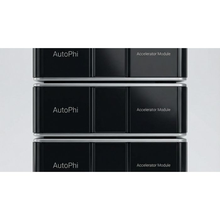
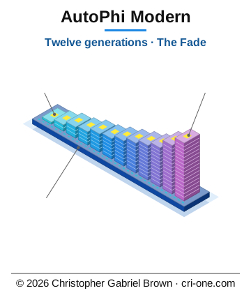
The roadmap moves on two curves: the process node fades down while the die grows thicker, from a tenth of a millimetre in the first generation to twelve millimetres and more than three thousand layers in the last. On-die electromagnetic Peltier cooling in every layer, with no external chillers, and LED recycling of waste heat back into current are what make the height possible. The first-generation eight-card chassis is rated above 2.8 zettaflops; the twelfth is listed at 18,000 times that.
It is for datacenter operators and chip licensees who want a compute line to tape out now and extend for decades. The buyer walks away with the RTL, the layouts, the synthesis results and the toolchain; the instruction set and the February 2026 patent application stay with Christopher Gabriel Brown.
Description
Patent status: Protected under U.S. Patent Application No. 19/540,453 (filed 13 February 2026). Additional applications pending: 19/445,644 and 19/449,352. Thirty further patent claims filed covering LED Power Recycling (Patent 3561/1026), Electromagnetic Cooling (Patents 1096–1098), Vertical Threading, Chiplet Stacking, Nanophotonic Data Flow, Quantum Error Correction, Quantum Battery Layers, Quantum-Classical Hybrid Execution, Neuromorphic AI Engine, Voxel Cell Architecture, and the multi-generation Fade stacking process.
Status: Active development — Year 1 (2026). Twelve-generation roadmap through 2063.
Overview
AutoPhi Modern is a complete, self-contained AI compute platform spanning twelve generations (APM01 through APM12) from 2026 to 2063. Each generation contains ten purpose-built processors — GPU, CPU, DPU, AI training, AI inference, computer vision, LLM engine, neuromorphic, quantum-classical hybrid, and edge — all running the original AutoPhi instruction set with nine Ultimate Technologies integrated on-die. That is 120 chip designs in total , backed by 76 Verilog source files (635,325 lines of RTL), 125 pre-generated GDSII tape-out files, 11 Yosys synthesis outputs, and a full open-source EDA toolchain.
The AutoPhi ISA is entirely original: Light Trigger photon-initiated execution, Color Mathematics wavelength-encoded ALU (Red = ADD, Orange = SUB, Yellow = MUL, Green = DIV, Blue = LOAD, Indigo = STORE, Violet = BRANCH, UV = QUANTUM), and a 16-instruction quantum gate set (H, X, Y, Z, S, T, CNOT, CZ, TOFF, SWAP, RX, RY, RZ, MEAS, PREP, BARRIER). No third-party ISA licence. No ARM, x86, or RISC-V dependency. Zero royalty obligations.
The Fade — Process-Node & Vertical-Stacking Roadmap
Performance scales through two smooth, opposing curves: process node fades down while die thickness fades up. Per-layer EM Peltier cooling (Patents 1096–1098) and LED Recycle Power (Patent 3561/1026) enable the height progression. Layer pitch shrinks with process: ~8 µm at 7 nm, ~6.5 µm at 5 nm, ~5.5 µm at 4 nm, ~5 µm at 3 nm, ~3.5 µm at 2 nm.
Total die area: 1,462 mm² across ten chips. Full chipset COGS at volume: $230 . Combined 8-card chassis: 2.8+ ZettaFLOPS .
1 LED Power Recycling 90% recycling efficiency; 42% net power reduction. On-die LED elements convert waste heat photons back to electrical energy. Scales to 85% net reduction at 3,430 LED surfaces (APM12). Patent 3561/1026
2 Vertical Threading 12,000 TSVs/mm² (APM01), scaling to 2,000,000 TSVs/mm² (APM12); 125 TB/s bandwidth. Through-silicon vias for 3D die stacking and inter-layer data flow. Patent pending
3 Chiplet Stacking Up to 500 layers (APM01); up to 3,430 layers (APM12). Multi-die vertical integration for compute and memory density. Patent pending
4 Nanophotonic Data Flow 1,400 TB/s per link; 2,800 WDM channels. O-band silicon photonics (1260–1360 nm). Scales to 910 PB/s per link at APM12. Patent pending
5 Quantum Error Correction 99.998% logical fidelity at distance-7 surface code; 1 MHz QEC cycle rate. 256 logical qubits (APM01-Q), scaling to 1,536,000 logical qubits (APM12-Q). Patent pending
6 Electromagnetic Cooling 97% efficient on-die EM Peltier; 32 independent thermal zones. No external chillers. Scales to 99.9% efficiency at APM12. Patents 1096–1098
7 Quantum Battery Layers 20 battery layers; 1,500 Wh capacity; 75 MW burst. On-die energy storage for instantaneous power delivery. Scales to 5,600 battery layers at APM12. Patent pending
8 Quantum-Classical Hybrid Shared register file between classical and quantum pipelines. Single-cycle handoff. Seamless integration across the full layer stack. Patent pending
9 Neuromorphic AI Engine Leaky Integrate-and-Fire spiking neuron model; 1,024 neurons × 8 synapses per neuron (base). Event-driven, near-zero idle power. Scales to 12,000M neurons at APM12. Patent pending
Voxel Cell Architecture — Three-Strand Encoding
The voxel is the fundamental building block of every AutoPhi die. Each voxel encodes computation in three parallel chromosomes processed simultaneously:
Strand Medium Encoding Purpose
Electron (Classical) Charge / current opcode, operands, result Conventional arithmetic, logic, memory
Atomic (Quantum) Qubit coherence gate_type, qubit_mask, phase, control Quantum gate execution, entanglement
Photon (Light) Wavelength / polarisation λ, polarisation, path, intensity Photon-initiated fetch/decode/execute, optical routing
Voxels tile into a 3D grid with six-way neighbour connectivity (N/S/E/W plus vertical TSV up/down). The voxel_cell Verilog module (138 lines) implements all three strands with concurrent execution and a shared cell register.
RTL Source — Shared Module Library
Ten synthesisable Verilog modules implement the nine technologies and the AutoPhi ISA as a reusable library instantiated across all ten chip designs:
Module File Lines Technology
Light Trigger Execution Core light_trigger_core.v 167 ISA — four-stage pipeline (Fetch/Decode/Execute/Writeback)
Color Mathematics ALU color_math_alu.v 114 ISA — 16 wavelength-encoded operations; FP64/FP32/FP16/BF16/FP8/INT64–INT4
Quantum Execution Unit quantum_exec_unit.v 154 ISA — 16-instruction quantum gate set with latency model
Voxel Cell voxel_cell.v 138 Foundation — three-strand building block with 6-way connectivity
Nanophotonic I/O nanophotonic_io.v 85 Tech 4 — 48-channel WDM transceiver; O-band 1260–1360 nm
QEC Surface Code qec_surface_code.v 60 Tech 5 — distance-7 surface code decoder; MWPM-based correction
EM Cooling Controller em_cooling_ctrl.v 55 Tech 6 — 8-zone proportional thermal management with emergency shutdown
Quantum Battery Controller quantum_battery_ctrl.v 65 Tech 7 — charge/discharge management; burst power delivery
Neuromorphic Engine neuromorphic_engine.v 88 Tech 9 — LIF neuron array with configurable synaptic weights
LED Power Recycler led_power_recycler.v 46 Tech 1 — 8-zone waste-heat harvesting with 90% efficiency
Total hand-written RTL: 972 lines across 10 modules. Synthesised netlist output: 598,671 lines across 10 netlist files. All synthesis performed by Yosys 0.58+138 .
Combined APM12 system (8-card chassis): 50,400+ ZFLOPS . Per rack (8 chassis): 403,200 ZFLOPS .
OpenLane2 Complete open-source RTL-to-GDSII flow (synthesis, floorplanning, placement, CTS, routing, signoff). Located in openlane2-main/ .
OSS CAD Suite 132 EDA tools for simulation, formal verification, and waveform viewing — Yosys, Verilator, SymbiYosys, GTKWave, nextpnr, and more. Located in oss-cad-suite/ .
GDSII Generator Standalone multi-generation GDSII generator for foundry handoff. Located in GDSII_GENERATOR_STANDALONE_CD/ .
Generation Script generate_generations.py (72,095 lines) — master source of truth. Regenerates all 11 generation directories (gen02–gen12) with chip specs, GDSII files, valuations, and roadmaps on demand.
02-autophi-quantum-processor Original Quantum Processor / REV accelerator with 30 patent claims, USPTO application, foundry handoff packages, and BGA-676 design rules.
05-quantum-battery Quantum Battery System — LED nano-charging, quantum dot arrays, foundry handoff.
10-autophi-accelerator-pcie-rev-h-rev-1 PCIe Gen5 accelerator card (Rev H, Rev 1) with manufacturing cost analysis and foundry handoff.
11-autophi-accelerator-microsdxc MicroSDXC form-factor accelerator — foundry handoff only.
12-autophi-accelerator-pcie-rev-h-rev-4 PCIe accelerator Rev 4 with peripheral chip, I/O signal array, and expanded chip designs.
14-semiconductor-material-discovery Alchemy Data V2 — top-2,000 compounds, RAG assembly, scoring algorithm.
17-autophi-accelerator-pcie-rev-h-rev-5 PCIe accelerator Rev 5 with USPTO image prompts and visual descriptions.
20-autophi-lower-cog-series Lower-COGS chip variations with tape-out-ready packages, material discovery, and manufacturing research.
21-autophi-manufacturable Manufacturability-focused design with 14 nm target, OpenLane runs, and foundry handoff.
24–27-autophi-scale series Scale CPU lineage — Scale (24), Scale Plus (25), Scale Pro (26), Scale Ultimate (27). Each with RTL, synthesis, OpenLane configs, testbenches, and GDSII outputs.
28-autophi-complete-unit Unified processor design that consolidates the Scale CPU and REV accelerator lines into a single chip.
1 High-Performance AI Acceleration System with PCIe Gen5 Interface and Custom TLP Processor Pending
4 AI Acceleration Core with Optimised Matrix Operations and Neural Network Processing Pending
GDSII tape-out files 125 pre-generated (10 APM01 + 110 across gen02–gen12), plus 120 standalone
RTL source + synthesis 178 MB 10 Verilog modules (common library), per-chip RTL, testbenches, 11 synthesised netlists, Yosys JSON outputs
OpenLane2 26 MB Complete RTL-to-GDSII flow with OpenLane2 configurations for all chips
OSS CAD Suite 1.9 GB 132 EDA tools — Yosys, Verilator, SymbiYosys, GTKWave, nextpnr, CVC4, and more
GDSII files 5+ MB 125 pre-generated tape-out files (10 per APM01, 10 per gen02–gen12) plus 120 standalone GDSII files
Chip specifications 143+ files Full specs for all 120 chips across 12 generations (per-chip .md with die area, layer count, PFLOPS, COGS, timeline)
Chassis specifications 2 files 8 server form factors with detailed BOM, cooling architecture, nanophotonic backplane designs
Documentation 373 files README, FIVE_YEAR_PLAN, VALUATION_SUMMARY, SALES_PITCH, IMAGE_PROMPT, roadmaps, foundry handoffs, patent receipts, lineage guides
Generator scripts 4 files generate_generations.py (master), generate_gdsii_all_gens.py, plus copy/migration scripts
Included project lineage 12 projects Scale CPU series (24–27), REV accelerator series (02, 10, 12, 17), MicroSDXC (11), Complete Unit (28), Quantum Battery (05), Material Discovery (14)
This package ships on a single Blu-ray disc, posted to the delivery address on your order. The archive on the disc is AES-256 encrypted; the passphrase is sent separately, by email, once the disc is despatched — so the disc alone is of no use to anyone who intercepts it.
Discs are despatched by tracked, signed-for post. Allow 5 business days for mastering and verification before despatch.
© 2026 Christopher Gabriel Brown. All rights reserved. Proprietary and confidential. Protected under U.S. Patent Application No. 19/540,453 (filed 13 February 2026). Additional patents pending: Application 19/445,644, Application 19/449,352. AutoPhi, AutoPhi Modern, Scale, REV, Complete Unit, Light Trigger, Color Mathematics, and The Fade are proprietary designations of Christopher Gabriel Brown.
Photo
Footnotes
- Product number 8446.
- Family: autophi core.
- Purchase: When you buy, you buy the use of that blueprint only.