
24-parts-future
Asset valuation: $2,000,000,000. Master index of all projects: PROJECTSINDEX. Last edited: 2026-05-02 Status: Generated 1,000-part catalog with full RTL + EDA output Maturity (per PACKAGEARCHITECTURE.md): L4 (Tape-out / Mass-Manufacturable) — full physical-design flow output present
Think of a seed catalog, except every seed is a chip. Parts Future is a generated catalog of one thousand IC part designs, each with its own SKU, specification and foundry handoff document, all grown from one architecture: the AutoPhi V18 voxel processor. The voxel is a compute cell, and like a biological cell it carries its plan as DNA - three strands rather than two. The electron strand is classical compute, the atomic strand is quantum compute, and the photon strand is light, with wavelength as the opcode and a single photon triggering each cycle. One logical step is written once and expressed in whichever strand carries it, so nothing is duplicated.
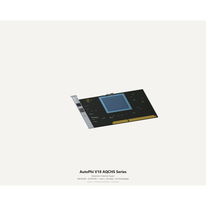
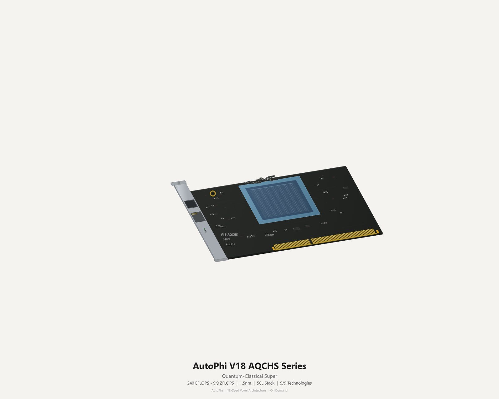
The catalog climbs ten tiers. At the bottom, fifty Seed parts at 130 nm, built for the SkyWater open PDK, with one of the nine core technologies active. At the top, eighty AQCHS parts at 1.5 nm for TSMC A16 or Intel 18A, carrying all eighteen photon opcodes from red ADD to indigo PHOTON_PIPE, all nine technologies from LED power recycling to a 3.20-billion-neuron neuromorphic engine, and reaching up to 9.90 ZFLOPS with ten million physical qubits. Every part number reads the same way: APV18, tier code, configuration number, process node. The archive is 25,584 files of RTL and full physical-design flow output. It is for the foundry buyer, the licensee and the engineering team that would rather pick a part off the shelf than design one. You walk away with the catalog and its handoff documents; the V18 architecture stays with the inventor.
Description
Parts Future — 1,000 Foundry-Ready IC Chip Designs
The Parts Future package is a generated catalog of 1,000 individual IC part designs , built on top of the AutoPhi V18 voxel processor architecture. Every part is a quantum–classical hybrid processor with a unique SKU, a complete specification, and a foundry handoff document. The catalog spans ten performance tiers from a $333 evaluation seed at 130 nm to a $2 trillion zetta-class complete unit at 1.5 nm. Total archive size: 25,584 files .
Architecture in brief: the 18-seed voxel DNA
Every part is an instance of the AutoPhi V18 architecture. The fundamental unit is the voxel — a compute cell analogous to a biological cell. Each voxel is specified by a three-chromosome DNA-style encoding :
Chromosome (strand) Physical carrier What it encodes Role
Electron (classical) Charge / current (opcode, operands, result_sink) Classical compute — ALU, registers, memory. Instruction width scales from 8 bits (Seed) to 512 bits (AQCHS).
Atomic / Quantum Qubit state (gate_type, qubit_mask, phase, classical_control) Quantum compute — rotations, CNOT, measurement, entanglement. Gate-type count scales from 1 (Seed) to 64 (AQCHS).
Photon (light) Photon — wavelength, polarisation, path, intensity (λ=opcode, pol=operand/phase, path=address, I=magnitude) Optical initiation and compute. Opcode count scales from 1 (Seed) to 18 (AQCHS). A single-photon light trigger initiates each cycle.
The three strands share one plan: the same logical step (e.g. “add A and B”) is encoded once and expressed in whichever strand carries it — photon (colour + intensity), electron (opcode + operands), or atom (quantum gate). The DNA-style idea is that a compact, replicable chromosome specifies computation without duplicating information.
The 18 photon opcodes (full set at AQCHS tier)
Each photon opcode maps a wavelength (colour) to an operation. Lower tiers activate a subset; the highest-tier parts carry all 18:
Each part activates a subset of the nine AutoPhi core technologies. Lower tiers activate 1–3; the Volume and AQCHS tiers activate all nine:
- LED Power Recycling — on-die light-to-electricity conversion, up to 90% efficiency.
- Vertical Threading — through-silicon vias (TSVs) for 3-D interconnect; up to 12,000 TSVs/mm² at top tier, sustaining 125 TB/s vertical bandwidth.
- Chiplet Stacking — multi-layer die stacking; from 1 layer (Seed) to 500 layers (AQCHS).
- Nanophotonic Data Flow — on-chip optical channels; from 0 channels (Seed) to 3,000 channels (AQCHS), sustaining up to 1,400 TB/s aggregate photonic bandwidth.
- Quantum Error Correction (QEC) — logical qubits derived from physical qubits via surface codes; fidelity from 93% (Seed) to 99.998% (AQCHS), error rate from 7% down to 0.002%.
- Electromagnetic Cooling — active on-die thermal management, up to 97% cooling efficiency at the top tier.
- Quantum Battery Layers — on-die energy storage; up to 20 battery layers, 1,500 Wh capacity, 75 MW burst.
- Quantum–Classical Hybrid — seamless interplay between classical ALU paths and quantum gate arrays within the same voxel grid.
- Neuromorphic AI Engine — event-driven spiking neuron arrays; from 0 neurons (Seed) to 3.20 billion neurons (AQCHS).
Complete 10-tier breakdown
Tier SKU prefix Parts Process node Price range (AES sell) Performance class FLOPS range Qubits (physical) Electron bits Photon opcodes Techs active Compute role Target foundry
1. Seed APV18-SEE 50 130 nm $333–$373 Kilo-class 100 KFLOPS–682 KFLOPS 1–4 8–10 1–2 1/9 CPU-only SkyWater (sky130, open PDK)
2. Micro APV18-MIC 70 130–90 nm $1.6K–$1.9K Kilo / Mega 709 KFLOPS–10.6 MFLOPS 4–19 10–13 2–3 2/9 CPU-only to CPU + light-GPU SkyWater / GlobalFoundries
3. Mini APV18-MIN 80 90–65 nm $7.7K–$9.2K Mega-class 11.0 MFLOPS–243 MFLOPS 19–84 13–18 3–4 3/9 CPU + light-GPU GlobalFoundries / TSMC
4. Entry APV18-ENT 100 65–45 nm $33.7K–$41.4K Mega / Giga 253 MFLOPS–12.2 GFLOPS 86–464 18–28 4–6 4/9 CPU + light-GPU to CPU + GPU GlobalFoundries / TSMC
5. Mid APV18-MID 120 45–14 nm $203K–$246K Giga / Tera 12.7 GFLOPS–1.34 TFLOPS 472–3,113 28–46 6–8 5–6/9 CPU + GPU to CPU + GPU + light-DPU Samsung / Intel / TSMC
6. Pro APV18-PRO 140 14–10 nm $1.21M–$1.56M Tera-class 1.40 TFLOPS–324 TFLOPS 3,161–25,073 46–82 8–11 6–7/9 CPU + GPU + light-DPU to CPU + full-GPU + DPU Samsung 14LPE / Samsung 10LPE / TSMC N10
7. Peak APV18-PEA 140 10–5 nm $7.45M–$9.61M Tera / Peta 337 TFLOPS–77.95 PFLOPS 25,440–182,182 82–147 11–13 7–8/9 CPU + full-GPU + DPU TSMC N7 / Samsung 7LPP / TSMC N5 / Samsung 5LPE
8. Unified APV18-UNI 130 5–3 nm $53.0M–$69.7M Peta / Exa 81.1 PFLOPS–12.69 EFLOPS 184,724–1,070,559 147–252 13–15 8–9/9 Full CPU + max-GPU + full-DPU TSMC N5 / Samsung 5LPE / TSMC N3 / Samsung 3GAE
9. Volume APV18-VOL 90 3–1.5 nm $422M–$508M Exa-class 13.2 EFLOPS–431 EFLOPS 1,085,000–3,530,531 253–367 15–17 9/9 Full CPU + max-GPU + full-DPU / All-in-one + Neuromorphic TSMC N3 / Samsung 3GAE / TSMC N2 / Intel 20A / TSMC A16 / Intel 18A
10. AQCHS APV18-AQC 80 1.5 nm $1.04T–$2.00T Exa / Zetta 448 EFLOPS–9.90 ZFLOPS 3,577,168–10,000,000 369–512 17–18 9/9 All-in-one + Neuromorphic / Complete Unit (all subsystems) TSMC A16 / Intel 18A
Total: 50 + 70 + 80 + 100 + 120 + 140 + 140 + 130 + 90 + 80 = 1,000 parts.
APV18 - SEE - 0001 - 130NM | | | | | | | +-- Process node (130NM, 90NM, 65NM, ... 1.5NM) | | +---------- Sequential config number, zero-padded (0001-1000) | +----------------- Three-letter tier code: | SEE = Seed MIC = Micro | MIN = Mini ENT = Entry | MID = Mid PRO = Pro | PEA = Peak UNI = Unified | VOL = Volume AQC = AQCHS +------------------------ AutoPhi Voxel 18 (architecture family)
Worked example: APV18-PRO-0500-14NM — AutoPhi V18, Pro tier, configuration number 500, fabricated on a 14 nm process node.
Example SKUs from each tier:
- APV18-SEE-0001-130NM — Seed #1, 130 nm, 100 KFLOPS, $333
- APV18-MIC-0051-130NM — Micro #51, 130 nm, 709 KFLOPS, $1.6K
- APV18-MIN-0121-90NM — Mini #121, 90 nm, 11.0 MFLOPS, $7.7K
- APV18-ENT-0201-65NM — Entry #201, 65 nm, 253 MFLOPS, $33.7K
- APV18-MID-0301-45NM — Mid #301, 45 nm, 12.7 GFLOPS, $203K
- APV18-PRO-0421-14NM — Pro #421, 14 nm, 1.40 TFLOPS, $1.21M
- APV18-PEA-0561-10NM — Peak #561, 10 nm, 337 TFLOPS, $7.45M
- APV18-UNI-0701-5NM — Unified #701, 5 nm, 81.1 PFLOPS, $53.0M
- APV18-VOL-0831-3NM — Volume #831, 3 nm, 13.2 EFLOPS, $422M
- APV18-AQC-1000-1.5NM — AQCHS #1000, 1.5 nm, 9.90 ZFLOPS, $2.00T
What is inside each part folder
Every one of the 1,000 parts has its own directory under parts/APV18-XXX-NNNN-XNM/ . Each directory contains five files :
File Format Contents
DATASHEET.md Markdown Full technical datasheet: specs table (process node, clock, FLOPS, TOPS, voxel grid, qubit counts, fidelity, error rate, memory bandwidth, nanophotonic channels, TSVs/mm², neurons, thermal zones, battery layers, LED efficiency, EM cooling efficiency, power, node performance multiplier, power/area reduction vs 130 nm); three-chromosome DNA architecture detail; active technologies list; performance analysis; competitive position; pricing and business metrics (IP valuation, COGS, sell price, gross margin, 5-year revenue projection, ROI).
spec.json JSON Machine-readable specification: every parameter from the datasheet in a structured format with typed values. Sections: specifications, node_comparison, technologies (9 boolean flags), pricing, foundry_handoff, competitive, meta.
FOUNDRY_HANDOFF.md Markdown Foundry submission document: target foundry, PDK, EDA flow, handoff status, submission steps, required deliverables (GDSII, LEF, DEF, gate-level netlist, DRC/LVS reports), RTL file list, IP valuation notes, compliance and NDA terms.
SALES_BRIEF.md Markdown One-page sales summary: headline, description, key selling points, target market, recommended applications, quick specs, competitive position, warranty and support terms.
README.md Markdown Part index: SKU, product name, tier, headline performance, process node, price, foundry, and file listing.
That is 5 files × 1,000 parts = 5,000 files in the parts/ directory alone.
Total archive file counts by type
The complete package (1,000 generated parts plus the AutoPhi V18 architecture substrate under 18-autophi-future/ ) contains 25,584 files :
(other) 616 HTML pitches, CSV catalogs, YAML configs, images, shell scripts, batch files, patches
- Master CSV — 18-autophi-future/1000_chip_sales_catalog.csv . One row per part. 74 columns covering: Config_ID, SKU, Model, Product_Name, Tier, Performance_Class, Sales_Headline, Full_Sales_Description, Key_Selling_Points, Target_Market, Recommended_Applications, all pricing fields (IP valuation, COGS, sell price, gross margin, revenue multiple, 5-year projection, ROI), foundry handoff fields (foundry, PDK, EDA flow, status, submission steps, deliverables, RTL files, summary), every technical specification, all nine technology flags, DNA architecture detail, competitive comparisons versus NVIDIA H100, and full performance detail.
- Build script — build_1000_parts.py (Python 3). Reads the master CSV, iterates over all 1,000 rows, and for each row generates five files in parts/APV18-XXX-NNNN-XNM/ . Functions: load_catalog() , make_datasheet(row) , make_spec_json(row) , make_foundry_handoff(row) , make_sales_brief(row) , build_all() .
- Architecture substrate — 18-autophi-future/ . Contains the AutoPhi V18 architecture: seed YAML, voxel configuration CSV (1,000 voxel configs), chip series definitions (CPU/GPU/DPU/All-in-one), OpenLANE2 seed design with completed runs (synthesis, place-and-route, STA, GDSII), Blu-ray build scripts, RAG source documents, and HTML pitch materials.
- Interactive browser — product_finder.html . Client-side catalog search and filter tool.
Process node range and performance scaling
The catalog covers twelve distinct process nodes : 130 nm, 90 nm, 65 nm, 45 nm, 28 nm, 14 nm, 10 nm, 7 nm, 5 nm, 3 nm, 2 nm, and 1.5 nm.
- SkyWater (sky130, open PDK) — Seed and early Micro parts. OpenLANE open-source EDA flow. Ready for MPW or shuttle.
- GlobalFoundries — Micro through Entry tiers.
- GlobalFoundries / TSMC — Mini and Entry tiers.
- Samsung 14LPE / Intel 14nm / TSMC 16FF — Mid tier.
- Samsung 10LPE / TSMC N10 — Pro and early Peak tiers.
- TSMC N7 / Samsung 7LPP — Peak tier.
- TSMC N5 / Samsung 5LPE — Peak and Unified tiers.
- TSMC N3 / Samsung 3GAE — Unified and Volume tiers.
- TSMC N2 / Intel 20A — Volume tier.
- TSMC A16 / Intel 18A — Volume and AQCHS tiers (most advanced).
Each foundry handoff document specifies: target foundry, PDK, EDA flow, submission status, step-by-step submission instructions, required deliverables (GDSII, LEF, DEF, gate-level Verilog netlist, DRC report, LVS report), RTL file list ( autophi_light_cpu_core.v , autophi_quantum_cpu_core.v , autophi_hybrid_cpu_top.v ), and the handoff summary.
Pricing and business model
- Pricing terminology: AES = Actual, tangible, bronze. AES COGS = actual cost of goods sold. AES Sell Price = real price to function.
- Gross margin: 40% across all tiers.
- Revenue multiple: 30× (used in 5-year revenue projections).
- IP valuation range: $1.0K (Seed #1) to $2.85T (AQCHS #1000).
- 5-year revenue projection per unit: $10.0K (Seed) to $60.0T (AQCHS).
- ROI: 67% across all tiers.
- Pricing tiers: AES Tier 0 (Evaluation, $500–$5K) through the highest AQCHS band.
- Performance: 9.90 ZFLOPS peak; 35,000 TOPS AI acceleration; 16.0 GHz clock.
- Voxel grid: 4096 × 4096 = 16,777,216 voxels, 500 stack layers, 28 stack units of 18.
- Quantum: 10,000,000 physical qubits; 3,500,000 logical qubits (QEC); 99.998% fidelity; 0.002% error rate.
- Memory: 360 PB/s bandwidth; 3,000 nanophotonic channels; 12,000 TSVs/mm².
- Neuromorphic: 3.20 billion neurons.
- DNA encoding: 512-bit electron chromosome; 64 quantum gate types; 18 photon opcodes.
- Power: 270 kW; 32 thermal zones; 20 quantum battery layers; 90% LED recycle; 97% EM cooling.
- All 9/9 core technologies active.
- Foundry: TSMC A16 / Intel 18A.
- Price: $2.00T AES sell; $2.85T IP valuation; $60.0T 5-year revenue projection.
- Compute role: Complete Unit (all subsystems).
- Performance class: Zetta-class.
Intellectual property
- Inventor: Christopher Gabriel Brown.
- Company: AutoPhi / CRI-ONE.
- Patent applications: USPTO 18/370,908 (quantum-battery + propulsion IC); 19/540,453 (Integrated Technology Portfolio, umbrella); 29/839,062 (design application, filed 2022-07-13).
- Classification: Proprietary / Trade Secret. Patent Pending on all novel architectural elements.
How this is delivered
This package ships on a single Blu-ray disc, posted to the delivery address on your order. The archive on the disc is AES-256 encrypted; the passphrase is sent separately, by email, once the disc is despatched — so the disc alone is of no use to anyone who intercepts it.
Discs are despatched by tracked, signed-for post. Allow 5 business days for mastering and verification before despatch.
Photo
Footnotes
- Product number 8472.
- Family: autophi on demand.
- Purchase: When you buy, you buy the use of that blueprint only.