Description
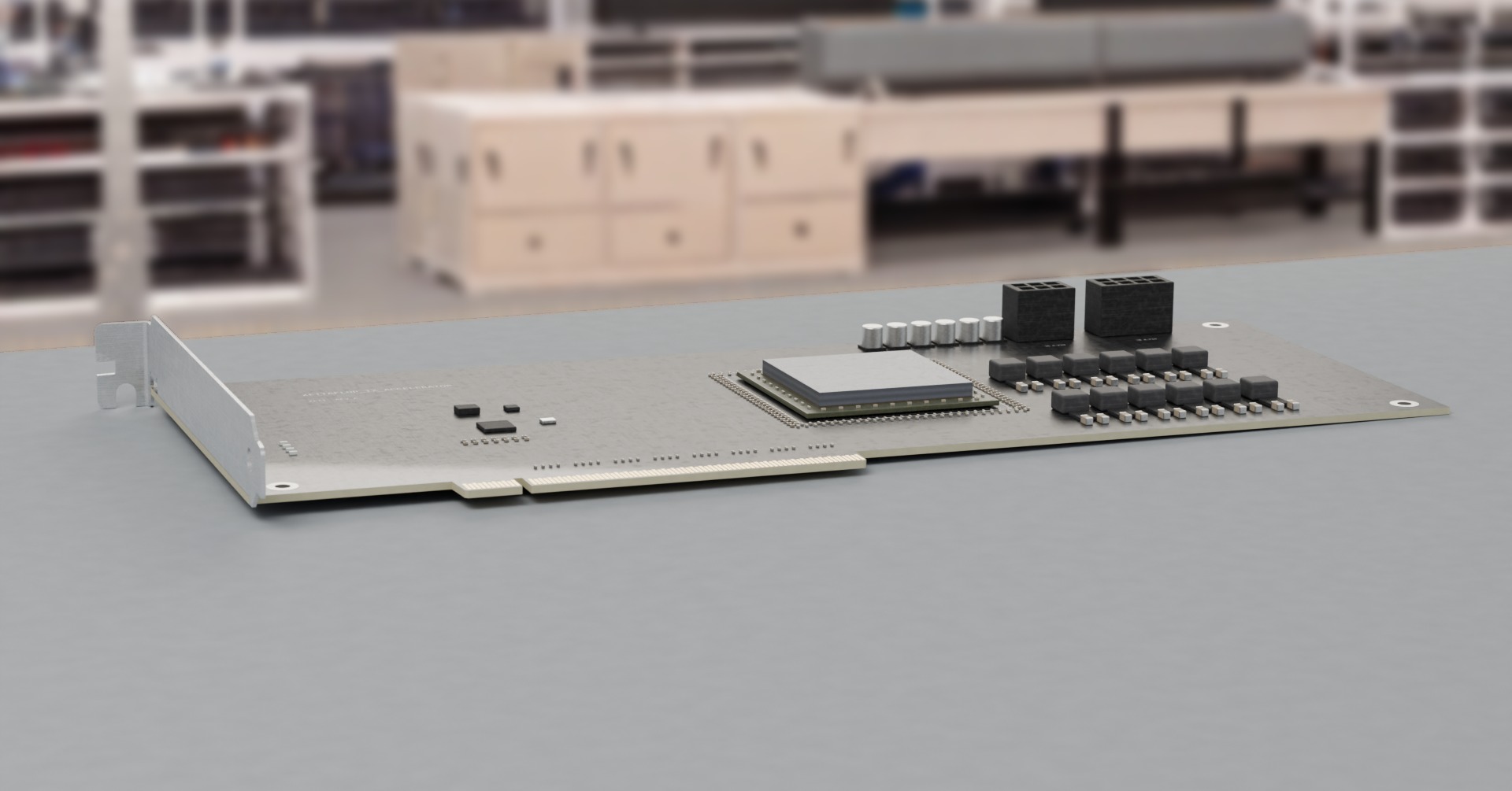
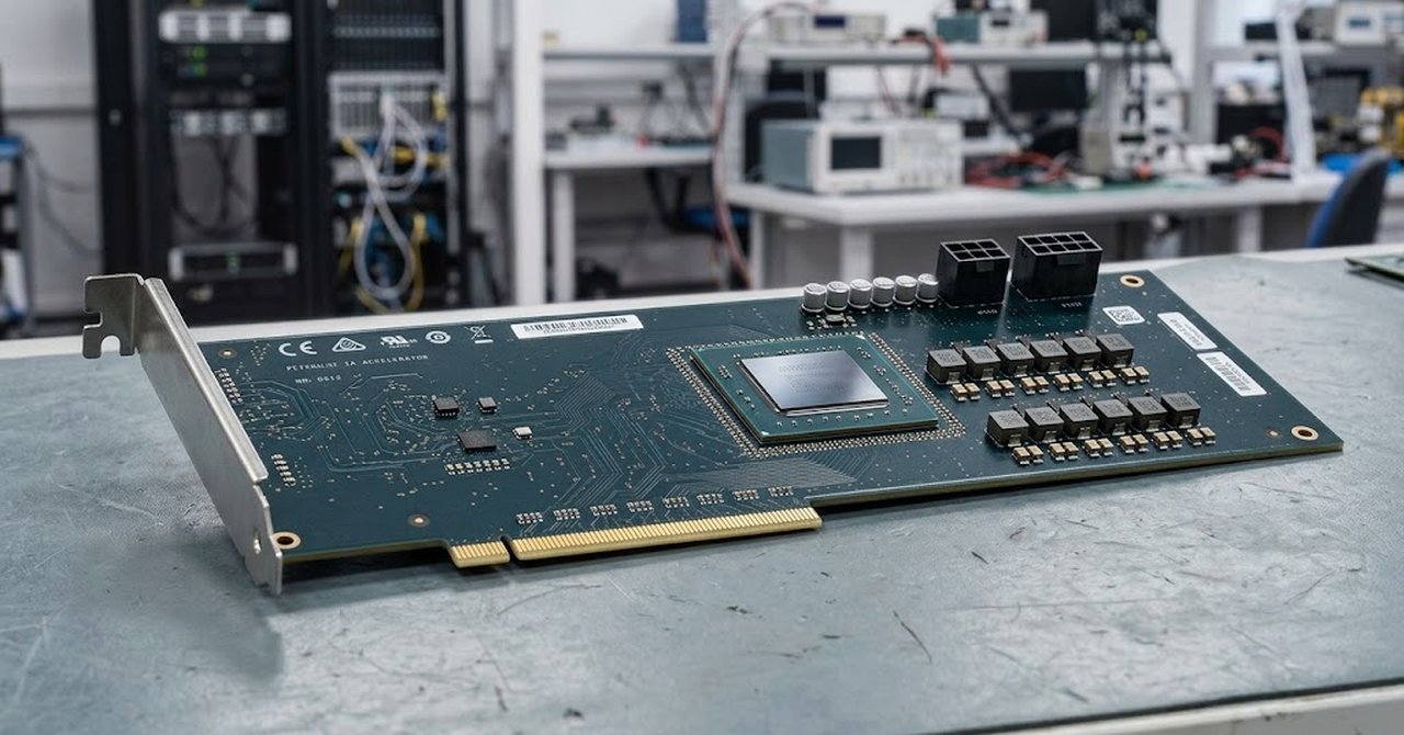
ZettaFLOP 1Z Accelerator — PCIe 5.0 Compute Card IP
Design ID: ZET1 (0x5A455431)
Patents: USPTO 18/370,908, 19/540,453, 29/839,062 (Light Trigger), 3561 2876 (Cold Light Micro Chip), 1026 (LED Recycle), 1096/1097/1098 (Electromagnetic Cooling)
Status: L4 Tape-out — 579/579 verification tests passing across 47 layers, foundry handoff package complete
Overview
The ZettaFLOP 1Z Accelerator is a PCIe 5.0 x16 compute card delivering zetta-FLOPS-class throughput from a single slot. The package bundles four sub-projects into one foundry-ready deliverable: AutoPhi Modern (Project 02 — 12 generations, 120 chips, APM01–APM12), AutoPhi Future (Project 18 — voxel-as-cell architecture with photon chromosomes), Communications Satellite (Project 19 — high-bandwidth I/O subsystem), and Day-One Fabrication (Project 21 — RTL-to-mask toolchain).
This is original silicon — not RISC-V, ARM, or x86. The architecture uses Color Mathematics, where colored light signals encode arithmetic operations. A single-photon Light Trigger initiates computation through digital micro mirrors and staircase mirrors for optical routing and temporal delay processing.
The Color Mathematics Instruction Set
Four wavelength-encoded operations, each processed through semiconductor lasers:
Color Hex Code Operation Performance Multiplier
RED 0xFF Addition 1x
BLUE 0x00 Subtraction 1x
GREEN 0x00 Multiplication 2x
YELLOW 0xFF Division 1x (with divide-by-zero protection)
The Light CPU core runs a 6-state pipeline: IDLE → TRIGGER → COLOR_DECODE → OPERATION → MIRROR_REFLECT → COMPLETE. Internal registers include an 8-bit light accumulator, 16-bit mirror delay counter (initialized at 100 cycles), and a 3-bit mirror angle routing output derived from the computation result.
64-Qubit Quantum CPU — 16 Custom Instructions
The quantum processor runs a 10-state machine (IDLE, DECODE, SECURE_INIT, QUANTUM_OP, MEASURE, ERROR_CORRECT, SANITARY_CHECK, SECURE_COMPUTE, VERIFY, COMPLETE) with configurable qubit count (64 default, supports 128+) and security levels 1–5. Fidelity: 95%+ maintainable, 99.75%–99.95% with Light Trigger assist.
Security Domain (4 instructions):
- QINST_SECURE_INIT (0x01) — Initialize secure quantum state
- QINST_SECURE_ERASE (0x05) — Cryptographic state erasure
- QINST_SECURE_TRANSFER (0x09) — Encrypted quantum data transfer
- QINST_SECURE_COMPUTE (0x0E) — XOR with 4 encryption keys, tamper detection via hash comparison
Performance Domain (5 instructions):
- QINST_QUANTUM_ADD (0x02) — Quantum addition via XOR
- QINST_QUANTUM_MUL (0x03) — Quantum multiplication via AND with entanglement
- QINST_QUANTUM_SEARCH (0x0A) — Grover-style quantum search
- QINST_QUANTUM_FACTOR (0x0B) — Quantum factorization
- QINST_ENTANGLE (0x0C) — Qubit entanglement
Sanitary Domain (4 instructions):
- QINST_SANITARY_CHECK (0x08) — XOR-based integrity hash validation
- QINST_ERROR_CORRECT (0x07) — Error correction (fidelity +5, error rate −2/−5)
- QINST_QUANTUM_MEASURE (0x04) — Measurement collapse to |0⟩
- QINST_QUANTUM_VERIFY (0x0F) — State verification
Advanced Domain (3 instructions):
- QINST_QUANTUM_COPY (0x06) — Quantum state duplication
- QINST_DISENTANGLE (0x0D) — Qubit disentanglement
- QINST_QUANTUM_VERIFY (0x0F) — Advanced state verification
Verilog RTL Module Hierarchy
Six synthesizable modules totaling over 1,200 lines of Verilog:
- ZETTAFLOP_1Z_ACCELERATOR_top — Top-level wrapper. Parameters: DESIGN_ID, DESIGN_VERSION, QUBITS=64, CLASSICAL_BITS=32, SECURITY_LEVEL=3, ACCELERATOR_TYPE=0, STACK_LAYERS=500, MAX_HEIGHT_UM=5000, LAYER_PITCH_UM=10. Contains all I/O declarations for CPU, PCIe 5.0 x16, all nine technology interfaces, MicroSDXC, and performance counters.
- autophi_scale_accelerator_integration (371 lines) — CPU-Accelerator bridge. 512-bit data packing/unpacking, memory request/grant handshaking, accelerator instruction injection. Data packing format: quantum_result[31:0], color_result[39:32], operation_mode[41:40], quantum_state[105:42], total_operations[137:106], with 382-bit padding.
- autophi_hybrid_cpu_top (158 lines) — Hybrid CPU integration. Instantiates both Light and Quantum CPUs. Coordinates operations, tracks light_ops_count and quantum_ops_count, generates combined completion signal, verifies security (secure_mode AND NOT tamper_detected), performance (ops count > 0), and sanitary status (sanitary_clean AND fidelity > 90%).
- autophi_light_cpu_core (177 lines) — The Color Mathematics engine described above.
- autophi_quantum_cpu_core (297 lines) — The 64-qubit processor described above. Internal registers: qubit_states array, entanglement_map, coherence_time (starts at 100, counts down), error_correction_level, security_hash, integrity_hash, 4 encryption keys (8-bit each), corruption_detector.
- autophi_accelerator_interface_adapter (207 lines) — Multi-protocol adapter. 5-state machine: IDLE, ADAPT_PCIE, ADAPT_SDXC, ADAPT_SET_OF_FIVE, WAIT_COMPLETE. Formats output for PCIe (512-bit for REV-1/4/5), SDXC (4-bit for MicroSDXC), or multi-chip (5 × 128-bit for Set of Five).
Five Accelerator Configurations
Accelerator Type ID Performance Memory Bandwidth Form Factor
REV-1 0 1.75 ZFLOPS 0.56 PB 40 PB/s PCIe 5.0 x16
REV-4 1 2.50 ZFLOPS 0.79 PB 56 PB/s PCIe 5.0 x16
REV-5 "Ultimate" 2 3.50 ZFLOPS 1.1 PB 78 PB/s PCIe 5.0 x16
MicroSDXC 3 512 GFLOPS 8 GB — MicroSDXC card
Set of Five 4 Combined — — Multi-chip (5 × 128-bit)
Performance Calculations
Scale-1 Baseline:
- Base threads: 268,435,456
- Stack layers: 62,515
- Clock range: 4 GHz (min) / 8 GHz (standard) / 16 GHz (max)
- Minimum FLOPS = 268,435,456 × 4 GHz × 1 op/cycle = 1.074 ExaFLOPS
- With Light Trigger boost (2x): 2.148 ExaFLOPS
- With mirror efficiency (40.82%): 877 PetaFLOPS standalone baseline
Scale-64 Maximum + REV-5:
- Base threads: 268,541,696 at 16 GHz = 4.297 ExaFLOPS
- With Light Trigger (2x) + GREEN Color Math (2x): 8.594 ExaFLOPS
- Combined with REV-5: 3.509 ZettaFLOPS
Comparison: Scale-1 CPU alone = 877x faster than NVIDIA H100. Scale-64 + REV-5 = 3,508,594x faster.
Physical Card Design
Parameter Specification
Card dimensions 268 mm × 111 mm
Die size per layer 36 mm × 36 mm (1,296 mm²)
Total layers 500
Layer pitch ~10 μm
Total stack height 5.0 mm
Total die area (all layers) 648,000 mm²
TSV density 12,000 TSVs/mm²
Chiplets per stack 18
Maximum stacks 28
Reflow profile Lead-free SAC305
Quality class IPC-A-610 Class 3 (high reliability)
ESD protection HBM 2000V, CDM 500V
JEDEC MSL Level 3 minimum
500-Layer Stack Architecture
Layer Range Function Count
1–200 Compute (Light + Quantum CPU) 200
201–350 Memory + Nanophotonic Interconnect 150
351–400 Vertical Threading + TSV Routing 50
401–450 Quantum Error Correction 50
451–470 Quantum Battery 20
471–490 Electromagnetic Cooling 20
491–500 I/O + Power Distribution 10
Nine Integrated Technologies — Full Specifications
1. LED Power Recycling (Patent 1026) — 90% photon capture efficiency, 42% net power reduction. 16-bit photon level sensing. RTL signals: ambient_light_level[15:0] , led_emission_level[15:0] , energy_harvested[31:0] , power_efficiency[15:0] (9000 = 90%).
2. Vertical Threading — 12,000 TSVs/mm², 125 TB/s inter-layer bandwidth. 18 data layers, 64-bit per layer. RTL: layer_data_in[63:0][17:0] , layer_data_out[63:0][17:0] .
3. Chiplet Stacking — 500 layers, 5 mm max height, ~10 μm pitch, 18 chiplets per stack, 28 stacks maximum. TSV bonding with nanophotonic waveguide alignment.
4. Nanophotonic Data Flow — 1,400 TB/s total bandwidth across 2,800 optical channels at 0.5 TB/s each. 256-bit per channel, 3 WDM wavelength control registers. RTL: photonic_data_in[255:0][2799:0] , photonic_data_out[255:0][2799:0] .
5. Quantum Error Correction — 99.998% accuracy, 1,400 logical qubits, 1 MHz error correction cycle, 32-bit per qubit data width. RTL: quantum_data_in[31:0][1399:0] , quantum_fidelity_accel[31:0] , coherence_time_status[31:0] .
6. Electromagnetic Cooling (Patents 1096/1097/1098) — 97% efficiency, 32 independent thermal zones, zero moving parts, near-zero power consumption. Target operating: 45–65°C. Max junction: 105°C. RTL: temperature_sensors[15:0][31:0] , cooling_control[15:0][31:0] .
7. Quantum Battery Layers — 20 layers, 1,500 Wh capacity, 75 MW burst power, integrated within the 5 mm stack. RTL: battery_charge_level[15:0] , battery_capacity[31:0] , discharge_rate[31:0] .
8. Quantum-Classical Hybrid Interface — Single-cycle handoff latency. 64-bit quantum data, 64-bit classical data, 64-bit result. RTL: hybrid_quantum_data[63:0] , hybrid_classical_data[63:0] , hybrid_result[63:0] , hybrid_ready .
9. Neuromorphic AI Engine — Near-zero idle power, event-driven activation. 32-bit spike interface. RTL: neuromorphic_spike_in[31:0] , neuromorphic_spike_out[31:0] , neuromorphic_ready .
PCIe 5.0 x16 Interface
- 16 differential pairs (TX + RX), 32 GT/s per lane, 512 GT/s total (64 GB/s)
- 100 MHz differential reference clock ( pcie_refclk_p , pcie_refclk_n )
- PERST# active-low reset
- 32-bit configuration space with 12-bit address
- Power: 75 W from slot + 225 W auxiliary (1 × 8-pin + 1 × 6-pin) = 300 W available
- Actual power required: ~140 W after LED power recycling — significant thermal margin
- Core voltage: 0.7–1.0 V (process-dependent), I/O: 1.8 V / 3.3 V
Memory Hierarchy
- 64-bit address bus, 512-bit data bus
- 3 memory types via 2-bit selector: 00=quantum, 01=photonic, 10=neuromorphic
- Photonic memory: 2,800 channels at 0.5 TB/s each
- Quantum memory: 1,400 logical qubits at 32-bit per qubit
- Neuromorphic cache: near-zero idle power, event-driven
- REV-5 maximum: 1.1 PB capacity, 78 PB/s bandwidth
Manufacturing Cost Breakdown (COGS: $91,300/card)
Component Cost
Wafer/Die (7 nm, 36 mm × 36 mm, 500 layers) $45,000
Memory Subsystem (photonic + quantum + neuromorphic) $12,000
Package Assembly (BGA, TSV bonding, nanophotonic alignment) $8,000
Quantum Battery Layers $5,000
Testing & QA (ATE, 579-test suite, burn-in, fidelity verification) $5,000
Electromagnetic Cooling $3,000
PCB & Card Assembly (signal integrity, power delivery) $3,000
LED Power Recycling $2,000
Overhead & Contingency (10%) $8,300
Year-1 list price: $150,000–$250,000 (39%–64% margin). Volume discounts: 10% at 11–50 units, 15% at 51–100, 20% at 101–500. COGS reduces 15%–25% at 10,000+ units/year. Lead time: 8–12 weeks after foundry fabrication. 1-year warranty standard (3-year and 5-year extended available).
EDA Flow
- Synthesis: Yosys — 4 scripts in synthesis/ , producing netlists in Verilog, JSON, and DOT graph formats (7 output files)
- Place & Route: OpenLANE — config.json , config.tcl , config_14nm.tcl , config_7nm.tcl
- Outputs: GDSII layout, SDC timing constraints, DEF placement, LEF abstracts
- SDC Timing: Input delay max 1.5 ns / min 0.3 ns (pcie_refclk domain), output delay max 1.5 ns / min 0.3 ns, false path on pcie_perst_n
- Automation: 4 shell scripts — generate_gdsii.sh , run_all_simulations.sh , run_openlane.sh , run_synthesis.sh
- Verification: 6 testbenches, 1 test vector file, 579/579 tests passed across 47 verification layers (100% pass rate, dated February 27, 2026)
Process Node Targets
Node Performance Range Purpose
130 nm 22–44 TFLOPS Proof run
14 nm 877 PFLOPS – 1.75 EFLOPS Production target
7 nm 877 PFLOPS – 8.59 EFLOPS Advanced target
Bundled Sub-Projects
- AutoPhi Modern (Project 02) — 12 generations, 120 chip designs (APM01–APM12), core RTL compute substrate. Includes 5-year plan, valuation summary, and the complete AutoPhi Unit (Project 28).
- AutoPhi Future (Project 18) — Next-generation voxel-as-cell architecture with photon chromosomes and Blu-ray foundry packages. 11 documentation files including deep-dive pitch, miracle calculation, processor power comparison, and seed voxel scaling analysis. 9 HTML pitch files.
- Communications Satellite (Project 19) — High-bandwidth I/O subsystem for the compute fabric.
- Day-One Fabrication (Project 21) — RTL-to-mask toolchain including the AutoPhi Scale accelerator integration module, verification report across all layers, and Python performance verification scripts.
What Is in the Package
- Source folder: 23-zetta-flops
- 137 total files (per MANIFEST.json): 73 documentation, 19 HDL (Verilog), 16 web (HTML), 5 EDA outputs, 4 data, 2 source code, 1 image, 1 layout
- 6 synthesizable Verilog RTL modules (1,200+ lines)
- 4 Yosys synthesis scripts with 7 netlist outputs
- 4 OpenLANE configurations (generic, 14 nm, 7 nm)
- GDSII layout + SDC/DEF/LEF foundry outputs
- 6 testbenches + test vectors
- Package specification: ZETTAFLOP_1Z_ACCELERATOR_package_spec.txt
- 10 architecture documents (including the ones detailed above)
- Complete patent reference file with prior-art analysis (scan completed 2026-05-11)
- CITATION.cff (CFF 1.2.0 format), CHANGELOG.md, hero image SVG
- Four complete sub-projects with their own documentation
How this is delivered
This package ships on a single Blu-ray disc, posted to the delivery address on your order. The archive on the disc is AES-256 encrypted; the passphrase is sent separately, by email, once the disc is despatched — so the disc alone is of no use to anyone who intercepts it.
Discs are despatched by tracked, signed-for post. Allow 5 business days for mastering and verification before despatch.
Footnotes
- Product number 8471.
- Family: autophi on demand.
- Purchase: When you buy, you buy the use of that blueprint only.